kamelfakihh
Newbie
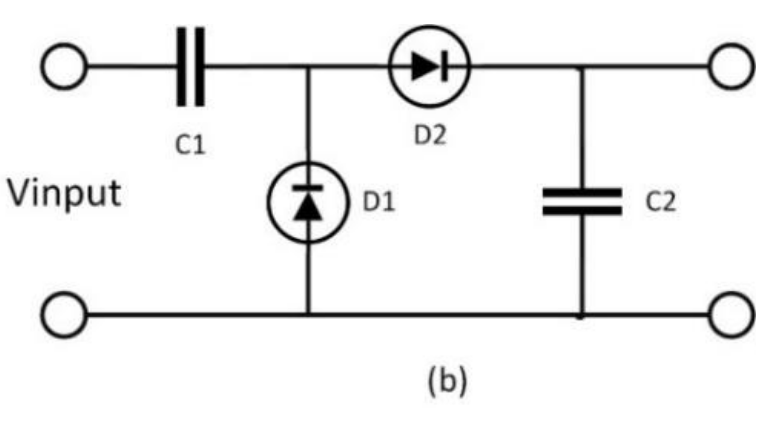
I am trying to replicate the rectifier/matching network design proposed in this conference paper on a different substrate (FR-4). The rectifier is based on the following voltage doubler circuit (using SMS-7630 schottky diode and 100pF capacitors, the circuit must operate at 2.4 and 5.8 GHz and the load impdeance is approx 3800 Ohm):

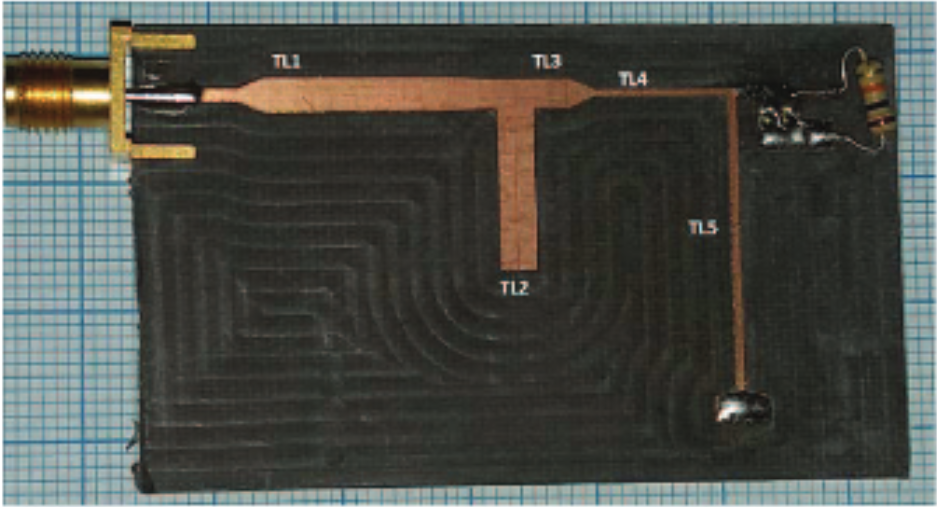
I'm struggling to understand the proposed matching network design (shown in the image below). It is not clear for me what is the role of transmission lines 4 and 5 and how did they find their dimensions. I do understand how does the T-section dual band impedance transformer (TL1, TL2, and TL3) work and I was able to calculate the line dimensions (based on these equations) and simulate the circuit in ADS without using the other 2 lines. However, the only issue was that the lines had high impedance values that I think are difficult to fabricate (W < 0.2mm)

I'm struggling to understand the proposed matching network design (shown in the image below). It is not clear for me what is the role of transmission lines 4 and 5 and how did they find their dimensions. I do understand how does the T-section dual band impedance transformer (TL1, TL2, and TL3) work and I was able to calculate the line dimensions (based on these equations) and simulate the circuit in ADS without using the other 2 lines. However, the only issue was that the lines had high impedance values that I think are difficult to fabricate (W < 0.2mm)