Continue to Site

Welcome to EDAboard.com

Welcome to our site! EDAboard.com is an international Electronics Discussion Forum focused on EDA software, circuits, schematics, books, theory, papers, asic, pld, 8051, DSP, Network, RF, Analog Design, PCB, Service Manuals... and a whole lot more! To participate you need to register. Registration is free. Click here to register now.

SMPS circuit

StraightView

Member level 1
Joined
Jul 7, 2023
Messages
37
Helped
0
Reputation
0
Reaction score
0
Trophy points
6
Activity points
455
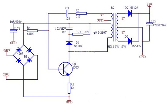
Hello everyone, I made three smps circuits copied from diagrams found in the internet like in picture below, but none of them worked, the problems I faced is either no current generated at transformer's output or as soon I connect the main power (220v), a short circuit happen and damaged the transistor or mosfet, I'm putting a single thin wire as a fuse, it gets burn out,
also according to my poor electronic knowledge, when I look to those smps diagrams I see that there's a short circuit of high voltage because the power goes directly to transformer's premary which is connected to transistor's collector and goes through the emitter which is connected directly to the ground! so is this not a short circuit?!!.
I appreciate any help solving this problem, thank you.
2021041414152920.jpg
 
Last edited:
No, it's not a short circuit. However, operating the SMPS power stage self-oscillating isn't likely to give reliable operation. To make it work at all, the circuit parameters have to be adjusted for the used components. I guess that's over your head.
 
No, it's not a short circuit. However, operating the SMPS power stage self-oscillating isn't likely to give reliable operation. To make it work at all, the circuit parameters have to be adjusted for the used components. I guess that's over your head.
Over my head?! How?!, I'm not completely ignorant about electronics, I have made successfully many, many circuits include similar circuits to smps like tuned oscillators, phase shift oscillators, inverter..... even thou I have never studied electricity/electrinics like in school, I faced a lot of problems making these circuits in the beginning, I tried to find some help in forums but I didn't get the help I needed like right here right now, so i counted 100% on my self and in the end I made it work, but for smps circuit I have just started to look how it works. Thank you for your help my friend.
 
The fundamental problem is that unlike most SMPS that have a control element, that design is self oscillating. If you look at almost every design it will have some kind of IC that contains a stable oscillator and a consistent drive signal to the transistor. They monitor the output voltage and adjust the drive signal to keep it constant.

The design you built relies purely on the feedback from the 9T winding to keep it oscillating and it will run at whatever frequency the transformers inductance and parasitic capacitances decide. It has nothing to monitor the output voltage and keep it stable. It works by the current through R4 turning the transistor on then (hopefully) the change in magnetic flux in the transformer is picked up by the 9T winding provides bias to keep it running. If you have reversed the connections to either primary winding or have insufficient signal coupling to the base pin, the transistor will just fully conduct and burn out.

Additionally, if the frequency it oscillates is higher than about 1KHz (and you should aim for about 50KHz), D1 will be too slow to turn on and off, it will probably cook.

Brian.
 
You need to show the detailed transformer design on here for any real help - the phasing is extremely important and you appear not to show it (?)

Tx construction is of vital importance too - not any old method will do

also the windings, turns, and core have to be just so to keep the flux bounded and to a reasonable level

If you have not successfully designed HF switch mode transformers before - then this will be an almost impossible task for you right now
 
The fundamental problem is that unlike most SMPS that have a control element, that design is self oscillating. If you look at almost every design it will have some kind of IC that contains a stable oscillator and a consistent drive signal to the transistor. They monitor the output voltage and adjust the drive signal to keep it constant.

The design you built relies purely on the feedback from the 9T winding to keep it oscillating and it will run at whatever frequency the transformers inductance and parasitic capacitances decide. It has nothing to monitor the output voltage and keep it stable. It works by the current through R4 turning the transistor on then (hopefully) the change in magnetic flux in the transformer is picked up by the 9T winding provides bias to keep it running. If you have reversed the connections to either primary winding or have insufficient signal coupling to the base pin, the transistor will just fully conduct and burn out.

Additionally, if the frequency it oscillates is higher than about 1KHz (and you should aim for about 50KHz), D1 will be too slow to turn on and off, it will probably cook.

Brian.
From your explaination I understand now what's the problem, you made it so simple and clear, thank you I appreciate your help.
 
You need to show the detailed transformer design on here for any real help - the phasing is extremely important and you appear not to show it (?)

Tx construction is of vital importance too - not any old method will do

also the windings, turns, and core have to be just so to keep the flux bounded and to a reasonable level

If you have not successfully designed HF switch mode transformers before - then this will be an almost impossible task for you right now
thank you for reply. I'm using ferrite transformer (picture below), I tested it with 300, 200 and maybe 100 hundreds turns of primary winding with two sizes very thin wire, one less than 0.1mm and the other also less than 0.1mm but larger than the first one, and auxiliary winding I tried with 20, 40 and maybe 60 turns with the same wire size of the primary, the secondary 20, 40,...... turns with wire of 1mm or more.
Notice, the coils in the picture are not what I'm talking about (smps) i have removed it, these transformer coils in the picture are for other circuit I'm working on.
IMG_20230708_073928.jpg
IMG_20230708_074027.jpg
 
Last edited:
First of all, the emitter is not shorted to ground ( hot ground that is ). There is a 12 ohm emitter resister. But you are essentially correct. The C1 capacitor is discharging 320V through a 12ohm resister when Q1 turns on. I guess at least 25A(peek) through Q1. 1N4007 diodes in the bridge are only rated for 1A so where is this 25A coming from anyway? I guess the pulse is short because you have only a 1uF C1 capacitor. Still a 25A pulse is probably too much for Q1. Maybe that resister should be more like a 180 ohm or bigger?

The other problem is that there is no output because the pulse is too short. The time constant of 1uF and 12 ohms means that your pulse is maybe 60us over a period of 100ms. And so the 320 volts gets reduced by the transformer winding ratio and the small pulse width down to 15mV of output. Even with a 180 ohm resistor you might get 2.2V out? You might have to fiddle with it, fine tuning the C1 size to get more output but not too much current to blow up things.

And what is that Q1 1303? Can it handle current? No clue what that is rated at. You need a transistor rated at 400V and that can handle the pulse current that you decide on. Probably best to use an enhanced mode MOSFET made for switching power supplies. It will have low RdON, a high switching frequency and made to handle high current pulses and high source to drain voltages.

Better of course to get a PWM controller chip as others suggested but I like the simplicity of the design for educational purposes. I might try it myself.
 
Do you have any idea about correct phasing of the windings ?
--- Updated ---

if not - google it
Correct phasing of the winding? I don't understand what you mean, it's simple, isn't?
I wrap the primary first around the core then i wrap it with tape, and then I wrap the auxiliary above the primary then I wrap it with tape, finally I wrap the secondary above them.
and for wires connection, is like the diagram, I connect one wire of primary to hight voltage input and the other wire to collector, for the auxiliary I connect one wire to transistor base and the other one to ground.
--- Updated ---

First of all, the emitter is not shorted to ground ( hot ground that is ). There is a 12 ohm emitter resister. But you are essentially correct. The C1 capacitor is discharging 320V through a 12ohm resister when Q1 turns on. I guess at least 25A(peek) through Q1. 1N4007 diodes in the bridge are only rated for 1A so where is this 25A coming from anyway? I guess the pulse is short because you have only a 1uF C1 capacitor. Still a 25A pulse is probably too much for Q1. Maybe that resister should be more like a 180 ohm or bigger?

The other problem is that there is no output because the pulse is too short. The time constant of 1uF and 12 ohms means that your pulse is maybe 60us over a period of 100ms. And so the 320 volts gets reduced by the transformer winding ratio and the small pulse width down to 15mV of output. Even with a 180 ohm resistor you might get 2.2V out? You might have to fiddle with it, fine tuning the C1 size to get more output but not too much current to blow up things.

And what is that Q1 1303? Can it handle current? No clue what that is rated at. You need a transistor rated at 400V and that can handle the pulse current that you decide on. Probably best to use an enhanced mode MOSFET made for switching power supplies. It will have low RdON, a high switching frequency and made to handle high current pulses and high source to drain voltages.

Better of course to get a PWM controller chip as others suggested but I like the simplicity of the design for educational purposes. I might try it myself.
Yes, like you said, it seems a short circuit especially these transformers used in smps has low resistance not like the iron transformers used in hight voltage, also resistor of 12ohm is like there's no resistance! I tried with 100ohm and get burn out immediately, also the circuit is acting as a savage short circuit when I connect the power, not like the components get heat up step by step and then burns out, I also tested it with power mosfet, it's the same result, I lost 3 or 4 mosfets, there's something wrong with that circuit, and the funny thing is I tried to make other smps circuits from other different diagrams than this one and non of them worked, in one of them the problem wasn't short circuit, it was no current at all in the transformer output.
 
Last edited:
Phasing doesn't mean the physical construction or size of the windings, it refers to the way the ends of the winding are connected. As with any transformer, if you reverse one of the windings, the polarity of voltage leaving it is also reversed. In your simplistic circuit the feedback needed to hold it in oscillation has to be in the correct polarity, the wrong way around actually stops it oscillating. It's the oscillating that produces the change in flux that results in the output voltage you want.

The principle of operation is:
AC line voltage is applied, it charges C1 and provides base current to the transistor through R4.
The transistor conducts and current flows through the primary (210T) winding.
As the current builds, some of the the changing flux is picked up in the feedback (9T) winding .
The current through R5/C3 flows into the base and turns the transistor off again.
When the current collapses, that through R4 takes over and the cycle repeats.

If the feedback winding is reversed, instead of its signal turning the transistor off, it tries to turn it on harder instead and this is what probably causes your problem. Try reversing ONLY the 9 turn winding, if you reverse the primary as well you achieve nothing and the polarity will still be wrong.

By convention, a dot is put on a schematic to identify one end of each winding so you know which way to connect them.

Also be careful that your secondary (8T + 8T) is wound correctly the winding should be 16T wound in the same direction with a tap in the middle.

I'm afraid DartPlayer170's diagnosis is misleading, it would only apply if the transistor was in permanent conduction and the circuit was dumping 320V straight across a 12 Ohm resistance. This would imply the circuit consumed about 850W ! In reality, if it worked it would only be a few Watts.

Brian.
Thank you again Sir, I have read in many electronic websites, forums and I personally didn't saw any one explain things like you do, as example, I personally didn't saw any one mentioning the fact about the winding polarity, (direction of the winding ends), in past I didn't think that it matters until I discovered by accident when I was working on tuned oscillator, but honestly I totally forget about it now working on smps, I will try reversing the winding ends of the auxiliary like you said, but with another smps circuit not this one in the picture, I got tired of it
 
Actually, I now see how this is supposed to oscillate. Because of the low C1 value I thought it was oscillating at mains frequency. But probably this won't work with this type of transformer. This is actually a modified schematic from an old ATX power supply's +5V standby circuit except that they modified it for 12V and removed the feedback stability for simplicity. There are a few problems with the redesign of this circuit however:

1 - C1 is too small. For some reason they reduced the size of C1 and this will prevent the circuit from oscillating. C1 is usually about 2X330uF in series. I would recommend using a 470uF 400V for this circuit. Otherwise C1 will discharge before the next mains cycle and the circuit will fail to oscillate.

2 - D1 is used as a snubber diode. 1N4007 is wrong. Bad design. This is a rectifying diode. Replace it with a high speed diode used for this purpose like a HER107G-AP. It has a reverse recovery time of 75ns and peek reverse voltage of 800V. The 1N4007 will fail to do its job and possibly result in damage to Q1.

3 - Not really clear what a 1303 is. But Q1 needs to be a high voltage switching transistor like KSC5027OTU.

4 - The transformer can be reused from an old ATX power supply that was used for the +5VSB. Just rewind the secondary with the same polarity and gauge but more windings. This will resolve the issue raised above about the polarity of the windings. The correct polarity in the control winding of the primary needs to be correct or else the circuit will fail to oscillate. You will also need to note the direction that the windings were used in the original circuit. If you wire them backwards, then it will once again not oscillate. The circuit is designed such that when C1 discharges through Q1, it causes the base of Q1 to begin to charge. If the timing is wrong, then it will simply oscillate at mains frequency.
I get tired of this circuit, I'm about to build another smps circuit, I will posted here after I finish. Thanks
--- Updated ---

I would guess 1303 is actually MJE13003.
Brian.
Some says that Q 1303 is 2SA1303 but I didn't used because I don't have it, I have used E13007F2 and two others their part number start by C i can't remember I got rid of them after they get burns out, but they are power transistors suitable for switching applications.
 
Last edited:
For anyone still interested, I found an old ATX power supply using the same circuit for the +5VSB. So, I disabled all the unrelated circuitries including the feedback that stabilizes the +5VSB. It works! 12.4V out with no load. The output is unstable with a load but nonetheless works and provides around 10V at 0.5A.

I am in Canada so mains here is 115V. Thus, the power supply has a switch and a voltage doubler circuit to get the 320Vdc across C1. So, C1 is 2 capacitors in series. 2 x 680uF @ 200V, equivalent to C1 of 340uF @ 400V. D1 is not a 1N4XXX series diode as expected. Not sure of the exact part as I cannot see it clearly. Q1 is a MOSFET, 4N60A. R1 is 4.7ohms as it is intended for 5V not 12V. C3 is 10uF @ 50V and R5 does not exist but there is a 56ohm resistor tacked on to the gate of the MOSFET. C4 is a 220uF @ 25V and only a single diode used on the output instead of a common cathode diode array. Another diode exists but it is used for the -5V, I believe.
 
2SA1303 has insufficient voltage rating and more importantly is PNP so it wouldn't work in that configuration at all.

I think the controversy about the low value of C1 is answered by it being the standby supply. It isn't intended to be used alone, C1 may be present but the source of input voltage will be the main PSU reservoir capacitors. I have never seen a computer PSU that duplicates the main rectifiers just to provide a low power standby supply or one that switches off power to the main rectifiers when in standby mode so it makes sense to keep them in circuit for both purposes.

Brian.
I finally managed to get the circuit to work, but not the first one I posted, I built another one (pictures below for more clarification).
Thank you Brian for the help I really appreciate it, and thanks to everyone here who tried to help.
In the beginning, I built the circuit as it is in the diagram (below), but after I connected the 220v to the circuit after that, nothing happened, but after a few seconds when I was about to measure it a short circuit occurred, and the wire that I put there as fuse burned out, and I found out that the transistor was super hot and damaged, and the 5.6v zener diode also burned out, so I made some changes and I succeeded, the circuit worked, I changed the R 330k to 1m, the capacitor 22uf/400v to 10uf/400v, and the 5.6v zener diode to another one I'm not sure of it's value, I measured the current by connecting the meter positive wire between zener diode and R 300 and the negative to ground and the reading was 4.somthing volts I can't remember.
I didn't use any of those transistors in the diagram, in the beginning I used E13007F2 which has damaged, in the second time I used C3150 transistor.

but there's some problems I would like to ask you about if you don't mind?
the transformer is making a loud noise, I have seen this issue before but I still don't know what caused it? and why?, from my guessing it's the high frequency, isn't?!,
also I would like to ask you about the role of the coils connected in series in the 220v input, and if the circuit can work fine without it?.
Last question and I'm sorry for these bunch of questions, if I want to increase or decrease the output power, can I do it just by changing the transformer values, or by changing the resistor values to increase or decrease the transistor switching rate?!!.
thank you again Brian.


iz_odv.png
IMG_20230710_172002.jpg
IMG_20230710_042608.jpg
IMG_20230710_042540 (1).jpg
IMG_20230710_042527.jpg
IMG_20230710_174212.jpg
IMG_20230710_042620.jpg
IMG_20230710_042627.jpg
IMG_20230710_042705.jpg
IMG_20230710_174247.jpg

2SA1303 has insufficient voltage rating and more importantly is PNP so it wouldn't work in that configuration at all.

I think the controversy about the low value of C1 is answered by it being the standby supply. It isn't intended to be used alone, C1 may be present but the source of input voltage will be the main PSU reservoir capacitors. I have never seen a computer PSU that duplicates the main rectifiers just to provide a low power standby supply or one that switches off power to the main rectifiers when in standby mode so it makes sense to keep them in circuit for both purposes.

Brian.
 
It is amazing you got this far with that very "open" layout - all the connections should be less than 1cm ( not joking )

and you need to heatsink the power transistor - else it will die pretty quick with any load on the output.

Also you need to research isolation on the transformer - not much fun getting a mains zap when you touch the output . !
--- Updated ---

also your C2 is the wrong way round ( in your sketch ) when compared to the original schematic and will go pop if you don't correct it.
Yes, the circuit now is a mess, I'll build it up nicely when I need to use it to run something, now it's just an experiment.
You are correct, I connected C2 wrongly.
Heatsink means connecting the transistor body to those aluminum pieces?.
 

LaTeX Commands Quick-Menu:

Similar threads

Part and Inventory Search

Welcome to EDABoard.com

Sponsor

Back
Top