arwen16
Junior Member level 3
Hello,
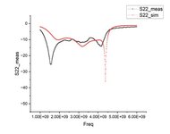
I had designed an LNA using an HBT from Infineon on ADS and had it fabricated and tested. The S11 measured was a good match with thr simulation results. However, the S22 measured looked like a flipped version of the S22 simulated. I don't know how to debug this issue.
I had designed an LNA using an HBT from Infineon on ADS and had it fabricated and tested. The S11 measured was a good match with thr simulation results. However, the S22 measured looked like a flipped version of the S22 simulated. I don't know how to debug this issue.