Continue to Site

Welcome to EDAboard.com

Welcome to our site! EDAboard.com is an international Electronics Discussion Forum focused on EDA software, circuits, schematics, books, theory, papers, asic, pld, 8051, DSP, Network, RF, Analog Design, PCB, Service Manuals... and a whole lot more! To participate you need to register. Registration is free. Click here to register now.

Question on charge pump or negative voltage supply

Status
Not open for further replies.

yschuang

Full Member level 3
Joined
Feb 1, 2004
Messages
183
Helped
15
Reputation
30
Reaction score
2
Trophy points
1,298
Activity points
1,002
Hello, all

I am reading an application note as follows.
www.intersil.com/data/an/an051.pdf
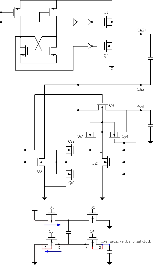
1. I was wondering how to turn off Q3 and Q4 with a voltage level translator.
Q3 or Q4 is turned off if Vgs,q3<Vt, which implies Vg,q3-Vs,q3<Vt. Vg,q3<Vt+Vs,q3. Vs,q3 is negatvie as I know. Therefore, Vg,q3 has to be
negative, too. Is that right and possible and how to implement that with a
voltage level translator ?

2. Am I right about drains and sources in each time ?
Fig. S1 represents one clock when S1 and S3 are on.
Fig. S2 represents another clock when S2 and S4 are on.
Drains and sources of Q3 and Q4 are on each figure and important because Q3 and Q4 require drive considerations like the application note said. Drains and sources are inverted each time. This is why i try to mark drains and sources in each time.


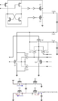
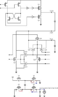
3. What is Qs5 for ?

Thanks
 

Hi, all,

Is anyone having answer or suggestion for these question? I have same questions in negative charge pump. How do I design a voltage level shifter to control the gate voltage to turn off Q3 and Q4? Should I use VOUT, the negative voltage output, for the VSS in level shifter?

Thanks!
 

Another question is:

How to implement the ESD protection? The forward bias diode will affect the normal operation.
What are the ESD structures using in this negative voltage output pin and ground pin?

Thanks!
 

I tried to answer these questions. However, I am not sure the answers are correct. I hope there is someone could help to discuss these questions.

1. From application note, the power and ground of voltage level translator are not VDD and VSS. It generates a voltage equal to the sum of the output voltage and supply voltage, and uses this voltage for the power of voltage level translator. And, it also generates an internal negative voltage(I think the voltage equal to the output voltage), and uses this voltage for the ground of voltage level translator. So, the crossing voltage for the voltage level translator could be controlled within VDD to avoid the break down risk.

2. I think it is correct.

3. Because the VOUT is chip interface, to consider the short circuit situation, the voltage of VOUT could be ground. So, we need to compare the drain, source, and ground to decide which one to connect to body.
 

In the older charge pumps the PMOS VT was well higher
than a diode Vf and tricky diode-blocked body schemes
might be employed. This becomes less viable in modern
technologies where "smart guys" push VT down for drive /
speed against a lower headroom.

These tricks are the "secret sauce" so you're not likely
to see them detailed in datasheets. Especially ones from
the present day. Thiis is where old paper databooks are
gold. Those "open" body terminals may or may not be
open. If open they may depend on natural body charge-
pumping to establish a +Vf (roughly) floating body back-
bias.

In a lower voltage / lower VT technology you might be
able to do similar things with a lower-Vf Schottky (if it
is suitably isolated).
 

Maybe I just can get some hints from patents not datasheet.

The open body means to float body, then uses the parasitc pn diode to automatically change the voltage of body to the more negative voltage of source/drain. Right?

Do you have any suggestion for the ESD?

Thanks!
 

Status
Not open for further replies.

Part and Inventory Search

Welcome to EDABoard.com

Sponsor

Back
Top