Continue to Site

Welcome to EDAboard.com

Welcome to our site! EDAboard.com is an international Electronics Discussion Forum focused on EDA software, circuits, schematics, books, theory, papers, asic, pld, 8051, DSP, Network, RF, Analog Design, PCB, Service Manuals... and a whole lot more! To participate you need to register. Registration is free. Click here to register now.

tactics for increasing charge /discharge of a system

yefj

Advanced Member level 4
Joined
Sep 12, 2019
Messages
1,208
Helped
1
Reputation
2
Reaction score
3
Trophy points
38
Activity points
7,254
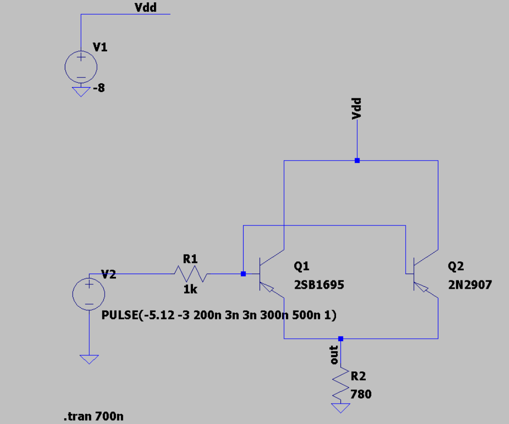
Hello,I have the following circuit where my output is on the buttom call out net.
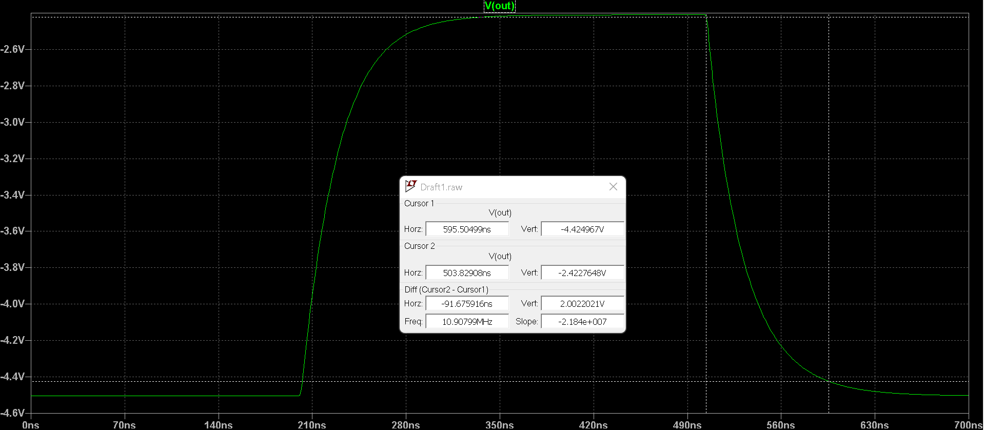
as you can see my out pulse has a very big charge and discharge time.
Is there a way to make the out pulse charge and discharge faster?

Thanks.
1712515179687.png


1712515157137.png
 
Hello Brain, This is exactly what i am doing now.
could you please give me an intuition regarding why exactly capacitor in parralel drastickly lowers the chargin and discharging?
How can i investigate the effect of this capacitor on input impedance to know the effect of rise and fall of the signal.

Thanks.

1712515807807.png


1712515845175.png
 
Last edited:
You are using medium power transistor 2SB1695 with relative large Ccb at low current which causes the observed waveforms.

Major deficite of the simulation is that it omits any load.
 
Hello FVM,given the capcitance model could you give me mathematical intuition regarding why adding this capacitor drasticly reduces the charge and discharge of the model?

1712591670102.png

1712591721424.png

1712591780045.png
 
Also consider the GBW.

If you see a risetime T(10~90%) where T=0.35 /f(-3dB) , compute your f BW and then check GBW of device and ask yourself, what is the gain for this circuit with load and parasitics, then what can you do to meet your goal. e.g. CB configs give the most BW with base AC grounded and low Re input impedance. Z(f)base / hFE). This essentially modulates Vbe to control Ic from the emitter Ie*Rsource. ECL uses this method in old high speed logic now called CML.

Remember I told you to look up analog differential Amps using ECL?
Why are you still using" old-school" CE configs for high speed?
 
given the capcitance model could you give me mathematical intuition regarding why adding this capacitor drasticly reduces the charge and discharge of the model?
You see about 20 pF Ccb forming a voltage divider with R1 and C1. It produces the waveform shown in post #3, 80 % fast, 20 % slow RC rise.
 
2SB1695 Transistors Low frequency amplifier
Why you want to copy that?

That is a 1A but very high hFE (dc) ~300) thus higher V gain, lower BW = GBW/Av .

Use the optimum GBW current if you want more BW which means about 50% of rated current.
Remember all transistors structured like diodes and all diodes are "Varicaps" and all diodes increase C towards 0V and reduce with reverse voltage. So when forward biased Vbe capacitance is the same as 0V for Cin which about double for a negative bias like -3V (-5V is normally max for B-E jcn.)

So reduce Re to optimal current Pd on transistor.

But 0 Ohm source signal is unrealistic.
 
Last edited:
Hello, my rise time got realy good but my fall time is still problematic.(I tried to add a capacitor in parallel to R2)
Before changing bjt or removing one of them, is there any method maybe connecting a diode?

In the attached video and photo in the end the author proposes to use a diode structure called baker clamp.
If this idia could improve the fall time situation even further how do you recommend to connect the diode?
Thanks.

1712752108471.png


1712752520669.png
 
All diodes have capacitance [pF], which increases with diode size. (lower (Vf-0.65)/If~Rs and decreases with reverse voltage. Same for Vce(sat)/Ic= Rce and RdsOn*Coss= Tout or RdsOn*Ciss=Tin

Imagine for each diode "family" thereis some almost constant RC=Tau at rated current. R is the bulk or incremental R on V/I slope and C= C(0V).
Diodes that are special structure have low Ron and low C(0V) like TVS diodes for ESD protection and special materials like GaAs and others than Si. Same for FETs with advanced semi materials.


But remember Current Mode Logic (CML) is even faster ( or ECL) (some > 1 GHz also CMOS comparators and 74ALCxx 3.6V logic


For BJT's Cbe is same at Cbe(0V) but only reduces with -Ve bias upto max -5V
Cceo is about half Cbe(0V) at Vce= +5V (npn).

Capacitance causes your RC = Tau rate of change with voltage. dV/dt = I/C so increasing current speeds up rate with lower shunt C.
While increasing series C || R increase transition current.

Inductance , ditto with current.

Search for switching transistor with Cout<< 5pF and compare results.
If no specs, it's not great.

Same for diode across C-E use low pF.
BC817: Collector-Base Capacitance CCBO — — 12 pF VCB = 10V, f = 1.0MHz
not bad but not great


Then
Try lower voltage Baker clamp with Schottky diodes or very low current pF protection diodes.
--- Updated ---

Even Differential amplifiers like 2 PNP or 2 NPN with roughly constant current using some -0.7 bias ar efaster than Common Emitter CE single transistors. like yours.

Why?
Think of it as an Emitter Follower (CC) with unity gain high BW and low Re = Rin/hFE1 driving a common base (same input resistance Rin||Cb /hFE2 but with V gain Rc/Re at some higher current than used in front end Op Amps.
--- Updated ---

Note that I said dV/dt = I/C nd I have spoken about RC effects of semi's.

Now your cct. uses Re = 750 ohms.

What expectations do you automatically have if Re = 100 Ohms?

hFE, Ic , Zin , Tau=RC but Rin includes Re*hFE , Tr, Tf, Pd .

Consider each. ( repeating these considerations will make it automatic in future.)
 
Last edited:
When R1C= R2C2/hFE or T1= T2 You have a flat BW approx. with no awkward slopes.
10:1 scope probes do this to flatten a square wave calibration.

Source Rs is not shown., || means parallel, + means in series.

The emitter sees time constant from Ze = (Rs + Z(T2) || T1*hFE+Rs

While the input from source (Rs + Z(T1) || Z(T2)*hFE for time constants using Bode plots in the frequency domain. for break points.

Recall Z(T) = R || 1/(2pi f C) for any RC in parallel T = Tau

The attenuation to emitter follows Kirchoff's Laws for an impedance divider.

Then the V gain also follows Kirchoff's Laws from impedance a ratio due to impedance seen at emitter,

Av = Zc/Ze until clipped or saturated at some Ic current controlled by Vbe and choice of R1 and R2=Re

~ Not rigourous math but truncated for "Level 1" approximations. :(

edit

hFE = DC current gain
Hfe = AC current gain (incremental)

1712781547917.png


(corrections invited)
 
Last edited:
I searched for backup references https://www.wikiwand.com/en/Common_emitter and the other technologies I previously suggested.


Agenda • Transmitter circuits
• Current-mode drivers
• Voltage-mode drivers
• Slew rate control


Maxim's CML paper

1712811895927.png

Texas Instruments serial gigabit solution devices that have an integrated CML drivers.
FET CML Thesis https://www.google.com/url?client=i...sQFnoECAMQAg&usg=AOvVaw0TGAeItW3m3baNZ8F2OBRy

The choice of transistors in this IC technology as stated originally are low pF for each PN junction and between all 3 pins on a BJT including negative feedback capacitance aka Miller Capacitance for C-B.

The choice of any technology depends on all I/O specs, Rise/Fall times, Voltage, Current range, I/O impedance, transition frequency, fT.

This is not an answer to the original question. Just a heads-up that you are using the wrong parts for you expectations.
A better question will have all these specs and with options to include cost, complexity, availability, quantity.
 
Last edited:
You are using medium power transistor 2SB1695 with relative large Ccb at low current which causes the observed waveforms.

Major deficite of the simulation is that it omits any load.
Hello ,I could not find CCB in the datasheet.Is there a better datasheet i could find the CCB?

Also you you tell why CCB is important for the charge and discharge of the output pulse? the are other capacitance .
Why its the most significant?
Thanks.

View attachment 190013
--- Updated ---

Hello , given the data sheet below could you tell why 2N5771 is better then 2SB1695
Could you show what is the charge and discharge equivalent model capcitance so i could try and simulate and see the difference?
Thanks.
 
Last edited:
All diode and PN junctions have C and are distorting your square waveforms.

They are all significant. Ccb, Cbe, Cce (but not always given for reasons that should become obvious when you understand my rant below.) i.e. If you understand the important of low something or other and the spec is missing, move on to another part.
e.g ESR in e-caps. you won't find ESR specs in standard e-Caps, but they do give the equivalent from which you can estimate ESR. , because . . . they are not low ESR and 100x worse, but lower cost.

But Ccb effect aka "MILLER EFFECT" became famous when John M. Miller published over a century ago the amplified effects of negative feedback with capacitance on Triodes.

As I said before C also increases with power rating for ALL PN junctions but decreases with reverse bias in Vcb, so obviously you do not need or want that power transistor.

The person whoever designed that lab power amp was probably thinking, what if I pair a power transistor with a fast switching transistor, then I'll get the benefits of both. (NOT) Instead, it has the bad limitations of both as wired AND not diode OR.:cool:
--- Updated ---

published in 1920 http://web.mit.edu/klund/www/papers/jmiller.pdf
 
Last edited:
All PN junctions have parasitic capacitance from a semiconductor dielectric between effective parallel conductor area.

Do you need Ccb if you have Cibo? aka Miller Capacitance, well that depends on application.


This includes all BJT nodes and FET nodes. They can be shown as discrete or lumped with net effects on the output and used either way to compute effects on signal, but Cibo , Cobo may be easier. Similarily in FETs Ciss, Coss.

Below can be defined in various ways by many sources, but I follow Infineon's method of the 3rd lead grounded.

1712870764294.png


1712873763880.png


Subscript notation for CXYZ is below:

X={i,o} input or output node
Y= b for base Cibo means that the base is common to both "i+o"
Z={o,s} open or shorted other end, e.g. Ciss= input=gate ,source=common, drain=short


Cobo shud read,

Cobo = Ccb + (Cce x Ccb) / (Cce + Ccb)


1712873838843.png


Images shamelessly copied from Infineon App Note 024, but was redacted (!).


1712884746991.png


Any questions> (there ought to be)

Another redacted publication on the Miller Effect (!) or just a website cleanp (?)


2SB1695
1712891312798.png


BFP840FESDH6327XTSA1
.
1712900855072.png
 
Last edited:

LaTeX Commands Quick-Menu:

Part and Inventory Search

Welcome to EDABoard.com

Sponsor

Back
Top