Welcome to our site! EDAboard.com is an international Electronics Discussion Forum focused on EDA software, circuits, schematics, books, theory, papers, asic, pld, 8051, DSP, Network, RF, Analog Design, PCB, Service Manuals... and a whole lot more! To participate you need to register. Registration is free. Click here to register now.
hi
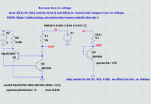
in the below pic, with simulation, it is seen that the turn-on voltage of Q1 is decreased from approximately 640mv to below 100mv.
explain what is the reason for it. how does pnp bjt (Q2) effect on turn-on voltage of Q1?
thanks
Your circuit description is given to misunderstanding. The original description is this "a circuit configuration with smaller forward voltage characteristics than that of a bipolar junction transistor (BJT) connected as a diode". You don't see Q1 turn-on-voltage rather than the forward voltage of an active diode circuit.
This experiment did not use a Voltage source for the NPN pullup resistor, thus no load current and not much voltage rise compared to the input voltage.
Observations for you to see
common base PNP is non-inverting
common emitter NPN is inverting
NPN-Vce will pull down Vb of PNP which pulls up Vb of NPN to saturate NPN Vce.
Vce will rise according to the difference between Vbe - Vbc = Vce (see plots of NPN)
If hFE2*hFE2 << Ic2/Ib1 it is saturating.
Rated saturation Vce(sat) in datasheets is given usually at Ic/Ib which is often <<10% hFE (DC current gain)
Thus Vcc for pullup on NPN becomes a comparator threshold to Vin. (if Rin/Rc<< hFE1*hFE2)
For PNP=Q1 , NPN = Q2,
Vbc1=Vcb2 So if NPN is not sinking current up thru 1k to Vcc, why is Vce= 20 mV? approx. in 3rd plot down for NPN.
With Vcc > 0V why does NPN pull down at Vin>=Vcc?
Interactive SIM with Vcc, and thumbwheel value changes. Beta = 50 constant (ideal)
Your circuit description is given to misunderstanding. The original description is this "a circuit configuration with smaller forward voltage characteristics than that of a bipolar junction transistor (BJT) connected as a diode". You don't see Q1 turn-on-voltage rather than the forward voltage of an active diode circuit.
Q2 is acting as level shifter compensating Q1 Vbe threshold.
I don't understand b.t.w. the test setup in the original Analog LTspice simulation circuit that uses an unipolar triangle waveform, also copied in post #1. I would suggest a bipolar stimulus to demonstrate rectifier operation.
With no load or pullup to the NPN, All the current comes the Sig Gen. Thus is appears to clamp any positive input to gnd. Yet with any loaf R to gnd on the output, it would block negative output from the input emitter being reversed.
Not a really a useful circuit, but it is unusual.
With a pullup resistor the PNP transistor has no effect.
This site uses cookies to help personalise content, tailor your experience and to keep you logged in if you register.
By continuing to use this site, you are consenting to our use of cookies.