Continue to Site

Welcome to EDAboard.com

Welcome to our site! EDAboard.com is an international Electronics Discussion Forum focused on EDA software, circuits, schematics, books, theory, papers, asic, pld, 8051, DSP, Network, RF, Analog Design, PCB, Service Manuals... and a whole lot more! To participate you need to register. Registration is free. Click here to register now.

Question about Momentum port setup for a transmission line simulation

Status
Not open for further replies.

sherry20

Junior Member level 3
Joined
Aug 18, 2009
Messages
29
Helped
0
Reputation
0
Reaction score
0
Trophy points
1,281
Location
N/A
Activity points
1,557
I'm running a simulation for a 50ohm transmission line in Momentum, and have been trying several ways to setup the port. This is an exercise for me to have a better understanding on how to set up simulations in Momentum.

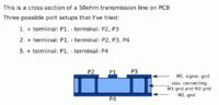
The structure is shown below. The signal line thickness is 52.5um, width is 635um, gap width on either side is also 635um. Dielectric thickness is 304um, epsilon_r=3.38. Bottom metal thickness is 35um, but in Momentum, it's set as a sheet.


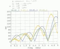
For the three port setup I tried, I got different results. What bothers me is the additional null shown in the case with 2 references.


My questions are:

1) Among the 3 port setups I've tried, what is the correct/mostly used way to set up a port in this type of problem?

2) Why is the additional null show up in one case but not the other two? The fact that it also shows up in the measurement makes me believe it's the correct answer out of the three. My guess is there's some parasitic mode being excited, but I can't provide a good explanation of the phenomena.

3) What could be some test cases which are easy to set up in simulation tool, and the theoretical solutions also exist? I try to get a few examples and try to match simulation with theoretical solution, so I can learn what the right ways are to set up the sims.

4) I'm new to the PCB extraction field, what would be some good ways to quickly learn about running EM simulation for PCB extraction? Is there any books/tutorial/forum thread etc that you're recommending? I have a computational EM background, but I realize a lot of subtle things are involved in PCB extraction and I need to catch up on that.

Thank you very much for any answers/comments you make.

Regards,

Sherry
 

You don't have to add P2,P3,P4 since you have a GND layer.P1 and ta the other side another Port let say P2 will be good enough.
Differential Odd Mode port configuration is only used when the GND layer is not present so RF return path is maintaned by side layer only.( Exiting + and - Ports are Odd mode)It's generally used in CPWG without GND ttype structures.

Thanks a lot for your help. If I only have P1 (and P2 on the other side of the line), when I setup port in momentum, the + terminal is P1 and - terminal is 'GND' (the theoretical ground of Momentum). I've tried this configuration and I got highly unphysical results, i.e. +20dB, so I thought there's something wrong.

Also, if I use +P1, -P4 vs. +P1, -gnd, what should be the difference?
 

I have simulated your structure and looks fine.The length of the TL is 100mm..

cpwg.PNGcpwg2.PNG
s11.PNGs21.PNG
 
Last edited:

I have simulated your structure and looks fine.The length of the TL is 100mm..

View attachment 109024View attachment 109026
View attachment 109027View attachment 109028

Oh wow! I can't believe you took the effort to draw and sim it! Thank you so much!

My actual structure is slightly different in the way that the two co-planar ground are much wider, ~ 6mm wide. and the length and width of the bottom metal layer is the same as the top layer, length = 61mm, width=14mm. Other than the difference in the numbers, I think it should work the same regarding passivity. I suppose you just dropped a pin there without doing any modification. Would the width of the co-planar waveguide cause trouble?

Thank you so much for your help, it's way beyond my expectation :)
Since the GND Vias are placed on the "Guide Strips", there will be a EM wall and therefore width of these strips have less importance.( Extreme cases are out of subject)I have simplified the structure in order to get the EM quick simulation results but nevertheless since the width of guide strips is as same as width of the TL, there is no sense to extend.
 
Since the GND Vias are placed on the "Guide Strips", there will be a EM wall and therefore width of these strips have less importance.( Extreme cases are out of subject)I have simplified the structure in order to get the EM quick simulation results but nevertheless since the width of guide strips is as same as width of the TL, there is no sense to extend.

I see. The weird thing is I keep getting the +20dB S11. Let me spend more time looking into it. If I still can't figure out what's wrong, I'll attach a workspace, maybe there's some stupid mistake I've made.

Thanks a lot!
 

I still haven't figured out what I did wrong here...I've attached my workspace, and I've run a few cases with different port setups, could you please take a look at it and tell me what I did wrong to get the unphysical result? Thanks you very much!

- - - Updated - - -

Since the GND Vias are placed on the "Guide Strips", there will be a EM wall and therefore width of these strips have less importance.( Extreme cases are out of subject)I have simplified the structure in order to get the EM quick simulation results but nevertheless since the width of guide strips is as same as width of the TL, there is no sense to extend.

Hi, I've attached my workspace in the above post, could you please take a look at it if you have time? I still get unphysical result, and my guess is there's a finite bottom ground below the transmission line. If I use an infinite ground, it would work, but my board is finite sized indeed.
 

Attachments

  • MyWorkspace1_50ohm_transmission_line.tar.gz
    12.6 MB · Views: 114

You did some mistakes..
*Don't put ports on guiding strips since they are tied to GND, let them be as they are..
*Don't use circular vias, instead use square vias to simplify the simulation setup
*Don't lay an extra GND plane underneath the MS Line because Momentum has a infinite and defined GND.It's an error..
*Look at my setup, it's simple and the results are meaningful.

Thanks, I see, the ground layer I have is probably causing all these troubles. Thanks a lot!
 

Status
Not open for further replies.

Part and Inventory Search

Welcome to EDABoard.com

Sponsor

Back
Top