Continue to Site

Welcome to EDAboard.com

Welcome to our site! EDAboard.com is an international Electronics Discussion Forum focused on EDA software, circuits, schematics, books, theory, papers, asic, pld, 8051, DSP, Network, RF, Analog Design, PCB, Service Manuals... and a whole lot more! To participate you need to register. Registration is free. Click here to register now.

RF Transmission line problem

Rimvis123

Junior Member level 2
Joined
Oct 30, 2023
Messages
21
Helped
1
Reputation
2
Reaction score
0
Trophy points
1
Activity points
190
Hello everyone,

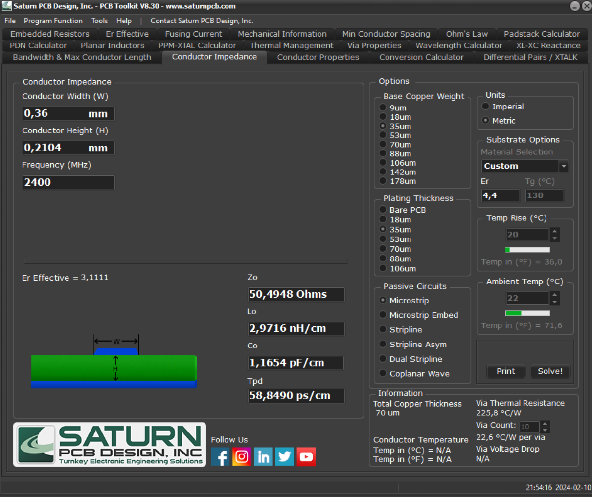
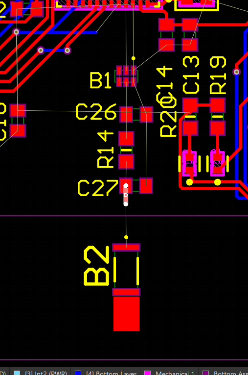
I'm using smd antenna with matching circuit ( R14 = L14) and i can't find optimal net width for 50 ohm impedance. If i'm doing it with saturn it shows me that net width need to be 0.36mm, but my matching circuit components footprint are much larger than that and if I use this width i could not reach 50ohm impedance in all line. So how to calculate it?
1707594882354.png

1707594911264.png


And this is my Stackup for this project (from JLCPCB 4 layer example)

1707594931214.png
 
Use smaller footprint. But this will not impact the Matching Circuit if the line is connected well up to SMD pad.
Because the model of those SMD Components have a Reference that is approx. Middle of the Pad.
 
But there should be a better way to do it, because these footprints are made by datasheets, so it's all ok with them and I don't wnat to make them smaller or use other. I saw videos from youtube how to do it, but most of them didn't work, because they are saying to add prepreg layer, but I don't know if JLCPCB can make it then.
 
But there should be a better way to do it, because these footprints are made by datasheets, so it's all ok with them and I don't wnat to make them smaller or use other. I saw videos from youtube how to do it, but most of them didn't work, because they are saying to add prepreg layer, but I don't know if JLCPCB can make it then.
0.36mm is not an issue.
 
I just asked my proffesor from university and he confirmed that, if I use 0.36mm net with matching circuit I will not get stable 50 ohm impedance because of matching circuit components, but he did not say any words how to solve it :) Maybe other will know how to fix it.
 
Generally speaking, component package parasitics (pad capacitance, series inductance) can be modelled and used to correct matching circuit component values. If you don't take package parasitics and also via inductance into consideration, the implemented matching will be far from designed value, particularly at > 1 GHz. Also expect large variations of actual trace impedance for thin FR4 prepreg. Usually component values have to be adjusted based on VNA measurement.

If you use 0402 L and C chips, effect of package parasitics can be reduced.
 
I just asked my proffesor from university and he confirmed that, if I use 0.36mm net with matching circuit I will not get stable 50 ohm impedance because of matching circuit components, but he did not say any words how to solve it :) Maybe other will know how to fix it.
He has probably meant that the matching components have already tolerances/temperature effects, therefore you should pay attention.
He may be right but 0.36mm can be manufactured precisely and you have to simulate ALL layout elements including SMD components with realistic models in a EM simulator. Then if you do a Monte Carlo Analysis with given statistical values, you can see how much deviation from the ideal case may occur.
For instance, a 0402 case Capacitor has 0.5mm width and you define PCB pad as 0.75mm (example) there will be approx. 0.35mm difference.
Its not so big.
 

LaTeX Commands Quick-Menu:

Part and Inventory Search

Welcome to EDABoard.com

Sponsor

Back
Top