Hawaslsh
Full Member level 3
- Joined
- Mar 13, 2015
- Messages
- 164
- Helped
- 5
- Reputation
- 10
- Reaction score
- 7
- Trophy points
- 1,298
- Location
- Washington DC, USA
- Activity points
- 3,422
I had a question about how much the transmission line to IC transition would affect my design in folks' prior experience. Typically when we make high frequency (up to 18 GHz) PCBs we use rather thin substrates (8 mil) and SMA end launch connectors with fairly thin center pins to match our transmission line width. With the thin substrate and fairly narrow line width, the transmission line width also tends to match (or come close to) the width of most ICs' pads. Below shows a picutre of what I am attempting to describe. The ground pour for the CPW is now shown, but there is a transmission line connecting to an IC's pad, and their widths are closely matched.

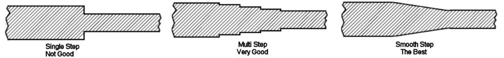
I am currently working on a board only to 7 GHz, and I wanted to use a much cheaper connector. One whose center pin is much wider in diameter (30 mils rather than 10). If I transition to a 20 mil substrate, I can create a 50 ohm CPW line with a width of ~30 mils (gap of 9 mil), matching that of the cheaper connector. Some rudementry HFSS sims a good return and insertion loss for a SMA to CPW tranistion up to 15 GHz with the 20 mil substrate and 30mil CPW width. However, this leads to my question. Despite my SMA to CPW transition being OK, now the transition from the wider transmission line to the IC looks really funky (shows below [the ground pour for the CPW isn't shown for simplicity]).

Using a line calculator, if you put in the dimensions of that IC's pad above (250um wide and 9 mil gap), you get about a 80 Ohm line/pad. I realize thats a very short length of pad, even compared to my highest frequency, 7 GHz (wavelength = 30mm @ 7 GHz for this CPW geometry). Am I over thinking this? Would this wide transmission line to IC transmission produce awful reflections?
I could simulate the transition from wide to thin transmission lines, but I am not sure how fruitful that would be. If anyone has any experience in this, any advice would be much appreciated
Thanks in advance
I am currently working on a board only to 7 GHz, and I wanted to use a much cheaper connector. One whose center pin is much wider in diameter (30 mils rather than 10). If I transition to a 20 mil substrate, I can create a 50 ohm CPW line with a width of ~30 mils (gap of 9 mil), matching that of the cheaper connector. Some rudementry HFSS sims a good return and insertion loss for a SMA to CPW tranistion up to 15 GHz with the 20 mil substrate and 30mil CPW width. However, this leads to my question. Despite my SMA to CPW transition being OK, now the transition from the wider transmission line to the IC looks really funky (shows below [the ground pour for the CPW isn't shown for simplicity]).
Using a line calculator, if you put in the dimensions of that IC's pad above (250um wide and 9 mil gap), you get about a 80 Ohm line/pad. I realize thats a very short length of pad, even compared to my highest frequency, 7 GHz (wavelength = 30mm @ 7 GHz for this CPW geometry). Am I over thinking this? Would this wide transmission line to IC transmission produce awful reflections?
I could simulate the transition from wide to thin transmission lines, but I am not sure how fruitful that would be. If anyone has any experience in this, any advice would be much appreciated
Thanks in advance