sabu31
Advanced Member level 1
Dear all,
I am testing PSFB for 48V output. At present the power level is around 400W, though system design is for 1500W.
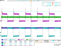
The primary and secondary side devices are SQW61N65EF. The primary side clamp diodes (D2, D4) are STTH3R06. At around 300V input the output is around 51 V and its starts to regulate.
However, after 10-20s , the D4 diode exploded. The ringing observed before the damage was within limits. However, when the system, was checked, though the devices did not show any heating or physically observable damage, the top devices of the primary and both secondary side devices were shorted.
In the bottom devices of the primary side, when the multimeter in continuity mode is kept in Drain to Source, there was a beep for some time (few secs) after which it showed OL (large). Similarly case happened when the probes of the multimeter were interchanged. The D2 diode was not damaged.
The resonant inductor used is 10uH primary side leakage is 7uH and magnetizing inductane is 3mH.
What is the reason for D4 getting damaged? Is it lower rated as compared to the requirement? Also is the MOSFETs getting damaged after D4 damage due to ringing. I am attaching the schematic.
Please suggest what should be done to resolve this and what is the recommended rating of the D2 and D4 diodes.
I am testing PSFB for 48V output. At present the power level is around 400W, though system design is for 1500W.
The primary and secondary side devices are SQW61N65EF. The primary side clamp diodes (D2, D4) are STTH3R06. At around 300V input the output is around 51 V and its starts to regulate.
However, after 10-20s , the D4 diode exploded. The ringing observed before the damage was within limits. However, when the system, was checked, though the devices did not show any heating or physically observable damage, the top devices of the primary and both secondary side devices were shorted.
In the bottom devices of the primary side, when the multimeter in continuity mode is kept in Drain to Source, there was a beep for some time (few secs) after which it showed OL (large). Similarly case happened when the probes of the multimeter were interchanged. The D2 diode was not damaged.
The resonant inductor used is 10uH primary side leakage is 7uH and magnetizing inductane is 3mH.
What is the reason for D4 getting damaged? Is it lower rated as compared to the requirement? Also is the MOSFETs getting damaged after D4 damage due to ringing. I am attaching the schematic.
Please suggest what should be done to resolve this and what is the recommended rating of the D2 and D4 diodes.