Continue to Site

Welcome to EDAboard.com

Welcome to our site! EDAboard.com is an international Electronics Discussion Forum focused on EDA software, circuits, schematics, books, theory, papers, asic, pld, 8051, DSP, Network, RF, Analog Design, PCB, Service Manuals... and a whole lot more! To participate you need to register. Registration is free. Click here to register now.

PSFB PCMC transformer saturation

Porsche

Member level 1
Joined
Jul 16, 2021
Messages
32
Helped
1
Reputation
2
Reaction score
1
Trophy points
8
Activity points
521
Hello everyone!
Recently I was researching my PSFB converter and came across a phenomenon that was unclear to me.

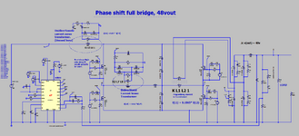
Please see schematic, it is classical PCMC PSFB. The current sense transformer (CST1) placed in sires with main power transformer T103.
Schematic_PSFB_2023-11-24.png

I configured error amplifier as a buffer such that a pot RP1 controls EAOUT voltage thus an effective duty cycle can be controlled manually by tuning RP1.

I noticed that when EAOUT (Red) signal reaches Sum(Green) signal, the shape of the current signal (Yellow) was greatly distorted. In the absence of "stabilization", the current shape looks normal and is almost the same for each cycle.

Please see following waveforms.

EAOUT (Red) has not reached sum signal (Green) at the ramp pin yet, thus maximum duty cycle observed (Blue - Tx's primary voltage). Current(Yellow) looks normal.
nogap-400v-15a-nostb.png


EAOUT(red) just touched the sum signal (green) and the current waveform fell apart. Nevertheless duty cycle has been limited (blue - the voltage on the transformer primary).
nogap-400v-15a-stbf.png


This kind of current shape distortion is very similar to the saturation phenomenon of the main transformer. But I have no idea how it is possible?
In the worst scenario, the calculated amplitude of the transformer magnetic flux density does not exceed +/-150 mT, which is almost 2 times less than the saturation limit of the N87 material (320 mT). The only reason I can think of for this, is that there is some DC current present in the transformer which pushes the hysteresis loop closer to saturation and then my +- 150 mT hits saturation point.

To confirm my theory I added a paper gap (0.1 mm) to the main transformer and indeed the current shape was not distorted anymore.

EAOUT (Red) has not reached sum signal (Green) at the ramp pin yet, thus maximum duty cycle observed (Blue - Tx's primary voltage). Current(Yellow) looks normal.
gap-400v15a-nostb.png


EAOUT(red) touched the sum signal (green) and the current waveform O.K. thanks to air gap. Duty cycle has been limited (blue - the voltage on the transformer primary).
gap-400v15a-stab.png


If the input voltage reduced under 200V it is possible to obtain a proper operation even without a gap in the transformer core.
nogap-200v15a-stb.png


I always thought that PCMC would prevent any core flux imbalance, but it seems it's not that simple.

Despite the fact that the gap in the transformer helped improve the situation, I would like to understand the reason for this process. I think that I have not solved the problem yet but just pushed it to a higher power level, which could lead to failure at extreme operating conditions. In addition, I have seen many appnotes in which the transformer has no gap at all.

Apart from introducing a gap, what is the correct way to solve this problem?

My magnetics data:

Primary transformer (T103) - ETD54 N87
Np = 24 Ns = 4

Resonant inductor (L101) - gapped RM 12 N87
N = 12 L = 22uH

Output inductor (L201) - APH40P60
Ae=1.072cm^2
Al=81nH/turn^2
le = 9.84cm
Bsat=1.5T
N=12
L = 10 uH (at the nominal load current)

Nominal input voltage 400VDC
Nominal power level 1800W
Fsw = 108kHz
 
Yes there is an answer - I wrote about it recently on linked-in

Need to know much more about the CT ( design ), its position relative to the main transformer, the load on the 4 CT diodes

and some information about the slope comp you are using to stabilise the system above 45% phase shift

there are lots of traps for newbies here
--- Updated ---

why is R6 in your ckt ? ( slope comp / curr sense )
--- Updated ---

We can't see the HVDC rail at the same time - this can be instructive also
--- Updated ---

if the secondary side of the transformer layout is assymetric ( imbalance of leakage L ) / messy - including through the diodes to the output caps, then you will get an imbalance of volt seconds referred to the primary,

esp if the forward drop of the output rectifiers is different - i.e. they are differently heatsunk

As we cannot see how you transformer is made, nor can we see the physical layout - we cannot comment further
 
Last edited:
why is R6 in your ckt ? ( slope comp / curr sense )
TI recommends adding at least 1V to the ramp signal to prevent asymmetry in CD pulses. Application Report SLUA275 - September 2002. So I am using 3 resistors to add 2/5 of the current signal, 2/5 of the compensation ramp, and 1/5 of the ref voltage (1/5*5=1V).
solution.png

Need to know much more about the CT ( design )
CT core is B64290-L45-X38, T38, R16х9.6х6.3, (Ae approx 20mm^2) 1 turn on the primary and almost 100 on the secondary. I also tried different materials (n87) but the signal shapes were the same on both CT's. The current transformer ring is located approximately 20 mm from the corner of the power transformer.
if the secondary side of the transformer layout is assymetric ( imbalance of leakage L ) / messy - including through the diodes to the output caps, then you will get an imbalance of volt seconds referred to the primary,

esp if the forward drop of the output rectifiers is different - i.e. they are differently heatsunk

As we cannot see how you transformer is made, nor can we see the physical layout - we cannot comment further
The secondary side of the transformer layout is as symmetric as possible, output diodes connected almost at transformer pins and caps are almost on the diodes. Diodes are on the same heatsink.
layout.png

Transformer is center-tapped and the secondary is made of copper tape. In total, on the secondary side there are 2 windings made of copper tape, 4 turns + insulation + 4 turns, a lot of insulation and the primary winding on top.

and some information about the slope comp you are using to stabilise the system above 45% phase shift
Is it possible that I have too much slope compensation to balance the flux or my output inductor is too small? Is there any rule of thumb for the ratio of the current slope / compensation slope?
 
I implore you to go to the LTspice simulator first......get it workigng in LTspice...only when you have it working there, do you go to the bench.

Simulator is not real...but there is a rule of electronics...."if you cannot get a representation working on the simulator first, then you will never get it working on the bench"
--- Updated ---

here is LTspice sim of PSFB
 

Attachments

  • PSFB_620V TO 290V 5A.zip
    4.4 KB · Views: 51
" 1 turn on the primary and almost 100 on the secondary "

sorry - how many on the secondary ? 50, 60, 70, 80 90 ?
--- Updated ---

The 1N caps across QC1, QD1 are likely excessive, try same as other leg
--- Updated ---

It does appear that your pri side current signal is being swamped by all the other crap you have piled on.

The CT checks out, assuming 90T, for 5A pk amp in the primary, you will get: 5 / 90T, *23 ohm = 1.277 volts pk

there is room to step this up quite a bit, e.g. 45 ohms would give 2.500 exactly - a much nicer number - and less noise

The slope comp to be added must be at least half of the down slope of output current referred to the pri side

We have at the moment 56Vout / 10uH = 5.6 A per uS is how fast the current will fall on the sec side in the dead times

referring to the sec side => x 4/24 = 933mA per uS, through the CT ( 90T ) and 45 ohms - this becomes => 0.466 V / uS

- but we need only half of this = 233mV per uS, or in the 45 ohm burden = 5.2 mA / uS extra in the burden to give the right slope comp.

If you want to use your extant ckt - you can do the calcs to level shift according to all the extra resistors you have thrown in.


Why have you tied CS to Ramp in the schematic ?
--- Updated ---

pins 9 and 10 could do with 4n7 to gnd right by their pins
--- Updated ---

. . . as could pin 2
--- Updated ---

make sure your CT / control ckt looks like this in reality on the pcb:

1700959457911.png


Also - you really should have a damping resistor associated with the diodes D105, 106 - you can see the horrendous current ringing you get without such R
--- Updated ---

you internal transformer construction is not really that symmetric - thus you will get different leakages on the sec wdgs when you short the pri

this is probably the fundamental cause of the flux walking in the Tx as it effectively providing different " drive " to each sec and hence a different reflected V.sec to the core on each half cycle.

Gapping the core is likely your best cure here - along with fixes listed above.
--- Updated ---

V ref can only supply 5mA - you have exceeded this is your slope comp buffer design.
--- Updated ---

also:
1700960258814.png


no more than 1uF - not the 4uF you show on your schematic
--- Updated ---

note also for Vdd:

1700960346896.png


10uF - right at the chip. as well as a chip cap !
--- Updated ---

Note also this:

1700960835321.png


R23 and or R29 are wrong value though.
--- Updated ---

Ooops - R31 or R 29
--- Updated ---

Finally - layout plays a huge issue and we cannot see the finished physical embodiment you have created.
 
Last edited:
I implore you to go to the LTspice simulator first......get it workigng in LTspice...only when you have it working there, do you go to the bench.

Simulator is not real...but there is a rule of electronics...."if you cannot get a representation working on the simulator first, then you will never get it working on the bench"
--- Updated ---

here is LTspice sim of PSFB
I have actually built a simplified model of my converter. Model was simplified in a sense that I have not modeled the exact PWM IC behaviour and feedback circuitry. Also as my basic model don't include modeling of the saturation phenomenon of magnetics it has little use now. I think I nedd to find UC3895 spice model first to improve my model.
sorry - how many on the secondary ? 50, 60, 70, 80 90 ?
97 turns on the secondary.
Why have you tied CS to Ramp in the schematic ?
Just for simplicity now. In real design I am using a voltage divider from RAMP pin to CS to fine tune current protection trip.
The 1N caps across QC1, QD1 are likely excessive, try same as other leg
At around 800W ZVS on QC QD was achieved. But I will put the same caps as QA QB to check if it is the reason for imbalance.
pins 9 and 10 could do with 4n7 to gnd right by their pins
Bypassing these pins to gnd creating a huge jitter in the gate signals and also greatly increase IC current consumption (+ ~20%). In the starting design I had 10n there. As soon as I removed caps, signals became stable like never before.
no more than 1uF - not the 4uF you show on your schematic
Oops... I will revisit these capacitors and increase summing resistors value to lower ref load.
Also - you really should have a damping resistor associated with the diodes D105, 106 - you can see the horrendous current ringing you get without such R
Since my D105,D106 is TO263 it will be pretty hard mod to do... I tried to add resistors in siries with these diodes on a previous PCB, but losses were just too high. And if these diodes can't affect on a symmetry in the primary current and just increase some EMI I prefer left it as it is for now.

If you want to use your extant ckt - you can do the calcs to level shift according to all the extra resistors you have thrown in.
My circuit is utterly simple. It contains 3 fixed resistors R4, R7, R6 such that R6=2R4=2R7. This gives us summing ratios of 2/5 of signal behind R4 (signal from CST), 2/5 of signal behind R7 (compensation slope), and finally 1/5 of the signal behind R6 (ref voltage). To keep everything simple these ratios are fixed. R6 gives us 1V of dc bias to the ramp signal and does not introduce any slope changes so it can be ignored.
Current sensor ckt.png

Originally, the compensation circuit I use can provide {2.5V}/{4.9μs} slope on the emitter of Q1. After summing only 2/5 of this slope are left, so 0.2 V/us is the maximum slope compensation value that can be added using these resistors values.
If we want added compensation to be at least half of the inductor current down slope, the inductor current down slope at the summing point must be no more than 0.4 V/us.
According to my calculations R17+Rp4 = 120 Ohm. In that case the amount of added slope compensation will be exactly 1/2 of the inductor down slope. But as I planned to work at much higher duty cycles than 50% I am greatly reduced R17+RP4 to make extra slope compensation to ensure no subharmonic oscillation even in D closer to 95%. I didn't find any info about too much slope compensation. So I decided more is better.
But revisiting these calculations sowed a seed of doubt in my mind. Maybe 23 ohm was an overkill in compensation. Your 45 ohms sounds like a much more reasonable choice. I will tune my RP4+R17 to 45 ohms.
And finally using a voltage divider I will feed a portion of this summed signal to the CS pin to make a current protection trip where I need it.

you internal transformer construction is not really that symmetric - thus you will get different leakages on the sec wdgs when you short the pri

this is probably the fundamental cause of the flux walking in the Tx as it effectively providing different " drive " to each sec and hence a different reflected V.sec to the core on each half cycle.

Gapping the core is likely your best cure here - along with fixes listed above.
I doubt there is such a thing as an ideal transformer in real world applications. There are no practical possibilities to make two windings exactly the same. There always will be differences in the windings or in layout.
Based on your experience, how often do you use a gap in transformers in your PSFB converters? Is introducing a gap a fairly common practice? I saw many appnotes describing PSFBs but nowhere was a remark considering flux walking prevented by a gap. The best I saw was "use high values of magnetizing inductance (no gap) for current mode control and low magnetizing inductance (with a gap) for voltage mode control" without further explanation why.

Finally - layout plays a huge issue and we cannot see the finished physical embodiment you have created.
I didn't post PCBs mainly because I have already made some changes to it. So It can be quite confusing. Please note, that the actual schematic is attached to the first post.
Main board.
PCB_PCB_A_V8_2023-11-26_top.pngPCB_PCB_A_V8_2023-11-26_bot.png
PCB_REAL.png
There are two current transformers on the primary wire. I used the second one to test how material will affect the waveform.
Please also note high res pdfs attached to this post.
 

Attachments

  • PCB_PCB_UCC3895_2023-11-26_top.pdf
    102.2 KB · Views: 61
  • PCB_PCB_UCC3895_2023-11-26_bot.pdf
    63.1 KB · Views: 50
  • PCB_PCB_A_V8_2023-11-26 bot.pdf
    290.3 KB · Views: 51
  • PCB_PCB_A_V8_2023-11-26 top.pdf
    394.2 KB · Views: 47
this is one of those builds where the devil is in the ( hidden ) detail - and we can't see clearly any build detail at all

The raw current signal out of the CT diodes would be very instructive - as then you can see the real current in the circuit - you appear to have 2 x CT's so the 2nd one could provide real Tx current signal only - ( the 2nd one must be shorted if not used )

For centre tapped secondaries - it is normal to put half on each side of the bobbin - not one over top the other - else the Tx will be very assymetric

The best case for the sec's is you use 2 lots of litz wire - bifilar with a twist - this guarantees each sec wdg looks the same to the pri wdg - having the same leakages, pri - sec1 & pri - sec 2, is very important for this topology.

It is a good idea to wind half pri - then secondaries, the final part of pri - to provide a low loss Tx and this also lowers the magnetic spray from the Tx.
 
Please see waveforms attached to the first post. Yellow signal is exactly the raw current signal out of the CT diodes, measured right at {R17+Rp4}.
 
@Porsche Did your problem got resolved? I am facing same issue. Same waveform of Transformer. If it is solved, can you please update, how it got resolved. Thanks in Advance!
 
@Porsche Did your problem got resolved? I am facing same issue. Same waveform of Transformer. If it is solved, can you please update, how it got resolved. Thanks in Advance!
Hello! Yes, I think I found the problem. The current transformer in series with the main Tx was the reason for the main transformer saturation. I think that DC current information was lost due to current transformer (CT) placement. This small DC current probably moved the BH curve of the main transformer closer to saturation. Since I replaced the current transformer and put it on the input bus, the problem has disappeared. I didn't change CT material, or slope compensation parameters. Just the placement of the CT makes a difference.

This placement of the CST1.1 leads to main Tx saturation.
Ct in ser.png
This placement of the CST1.1 works fine.
Ct in bus.png
 
Thanks for your reply. For my case CT is already on HV, not in transformer series. Still getting similar waveform but after 1 hour, when transformer heats.
 
Hi,
With great thanks to Easy Peasy, this has been a great thread on PSFB.
Out of it came the realisation that high power PSFB with split sec needs the two secs to be wound
side by side, not one atop t'other.
But also, and the attached is being adapted to suit the OPs spec, we can do the PSFB
with current doubler rectifier...in that case, we only need a single sec.
OK we have two output inductors at half frequency, but micrometals sendust etc can easily get us out of that one.
As you know the PSFB, in its best form, has big turn-off snubbers
across the FETs and the FETs are then turned off super quick....to reduce switching losses.

However, its well worth doing a PSFB even without this "extra".
This as we know, is becuase the PSFB does not suffer shoot through due to sudden duty cycle change of the
transformer gate drive...because as we all know , in a PSFB , the duty cycle of the GDT never changes...only its phase changes.

And i think we now have birth of a "new" SMPS...the "Jack PSFB"...basically a "Full Bridge with added leakage L and phase change gate drive" with the bonus that
you never get shoot through issue...(as long as you dont suddenly turn the GDTs off in some fault protection etc.
 

Attachments

  • PSFB_400V to 48V at 1800W.zip
    4.3 KB · Views: 29
  • PSFB 400V TO 48V at 1800w.png
    PSFB 400V TO 48V at 1800w.png
    98.5 KB · Views: 24
@Homeshpwe

we find most people under size the CT when they put it in series with the transformer, or, have it too close to a magnetic with fringing mag fields that really upset things, when they move it to the DC bus, it sees less V.uS, and it is further away from stray fields - hence better results.

Also a CT sitting right on a switching node can pick up noise from that switching node which then capacitively couples into the signal out - if no attempt is made to shield the wire going thru the CT !
 

LaTeX Commands Quick-Menu:

Similar threads

Part and Inventory Search

Welcome to EDABoard.com

Sponsor

Back
Top