Continue to Site

Welcome to EDAboard.com

Welcome to our site! EDAboard.com is an international Electronics Discussion Forum focused on EDA software, circuits, schematics, books, theory, papers, asic, pld, 8051, DSP, Network, RF, Analog Design, PCB, Service Manuals... and a whole lot more! To participate you need to register. Registration is free. Click here to register now.

NWELL_StampErrorFloat cadence

Status
Not open for further replies.

richaphy

Member level 1
Joined
Mar 20, 2012
Messages
35
Helped
1
Reputation
2
Reaction score
1
Trophy points
1,288
Location
Greece
Activity points
1,592
Hi
I am learning to use Cadence by designing an OTA.
I'm a bit stuck understanding what these error messages mean in the DRC checker.
if there is a link where I can find an explanation please let me know, otherwise I'd really appreciate some help understanding the following:

1. NWELL_StampErrorFloat
(NWELLs are highlighted)

2. Maximum N+ Diffusion to nearest P+ pick-up spacing (inside P-Well or T-Well) is 20um
all nmos diffusion highlighted

3. Maximum P+ Diffusion to nearest P+ pick-up spacing (inside N-Well or T-Well) is 20um
all pmos diffusion highlighted

I have connected the supply and groung to their respective connections int he nmos and pmos.

Also, just checking
Do I need to connect the bulk of each pMOS transistor to VDD, would this be the NWEL?
and the bulk of the nMOS transistors to VSS, would this be the substrate?
Which means here is it necessary to provide a guard ring??
I tried the guard ring as well but even with that the error1 is still there.
Thanks
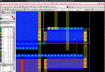
 

1. NWELL_StampErrorFloat (NWELLs are highlighted)
Similar to this thread's solution.

2. Maximum N+ Diffusion to nearest P+ pick-up spacing (inside P-Well or T-Well) is 20um
all nmos diffusion highlighted

3. Maximum P+ Diffusion to nearest P+ pick-up spacing (inside N-Well or T-Well) is 20um
all pmos diffusion highlighted

Maximum ... spacing ... is 20µm. Shouldn't this make it clear? Check your Design Rules!

I have connected the supply and groung to their respective connections int he nmos and pmos.
Good!

Do I need to connect the bulk of each pMOS transistor to VDD, would this be the NWEL?
Yes!
... and the bulk of the nMOS transistors to VSS, would this be the substrate?
Yes again!
Which means here is it necessary to provide a guard ring??
No!
 

Screenshot-7.png
Thanks for your reply.
I have attached a snapshot of the layout.
As you can see the distance between nplus and pluse diffussion is less than 2um. But still I am getting these errors.
2. Maximum N+ Diffusion to nearest P+ pick-up spacing (inside P-Well or T-Well) is 20um
all nmos diffusion highlighted.
3. Maximum P+ Diffusion to nearest P+ pick-up spacing (inside N-Well or T-Well) is 20um
all pmos diffusion highlighted
Also I want suggestion, I am making a design with some quiet long connection line with metal (around 50um long). What width I should choose for these line. Keeping in mind the things like parasitic like capacitance between two parallel connection metal line/wire.
Please help me to solve these issues.
Thanks
 

Your errors are for n+ diff to P+ pick-up (ie bulk connection) and p+ diff to N+ pick-up. Are you LVS clean?
 

I am not able to understand this bulk connection.
How can I connect bulk to ground or supply>>
Do I need to use guard ring??
Thanks

- - - Updated - - -

I think I got the answer, I have to draw a via M1 to Pactive and M1 to Nwell each for NMOS and PMOS respectively, which will be connected to ground and supply.
 

Your process may have dedicated layers to use for bulk ties. If not, use p+ diff and n+ diff to connect the bulks. Just quickly throw something down in the substrate and nwell and get LVS clean. After that, work on DRCs and tidy things up to your liking.
 

- - - Updated - - -

I think I got the answer, I have to draw a via M1 to Pactive and M1 to Nwell each for NMOS and PMOS respectively, which will be connected to ground and supply.

Right; not a via however, but a contact. Vias are connections between metal layers.
 

You should study some basic on semiconductor! Basiclly, MOS have 4 terminal include Sourece, drain, gate and bulk. As u mentioned bulk is ptap connected to psub and ntap connecnted to Nwell.

Other problerms are about DRC, you should learnt design rule firstly, and cleaned all errors.
 

Status
Not open for further replies.

Part and Inventory Search

Welcome to EDABoard.com

Sponsor

Back
Top