Continue to Site

Welcome to EDAboard.com

Welcome to our site! EDAboard.com is an international Electronics Discussion Forum focused on EDA software, circuits, schematics, books, theory, papers, asic, pld, 8051, DSP, Network, RF, Analog Design, PCB, Service Manuals... and a whole lot more! To participate you need to register. Registration is free. Click here to register now.

matching connector to microstrip question

yefj

Advanced Member level 4
Joined
Sep 12, 2019
Messages
1,192
Helped
1
Reputation
2
Reaction score
3
Trophy points
38
Activity points
7,199
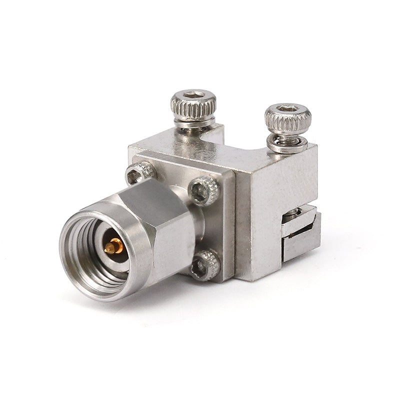
Hello I have a connector .we match 0.27mm microstrip trace to the connector using a taper.I know that a taper is transformer between impedances. given the connector shown below what kind of taper do you reccomend to build for proper transition of coax to microstrip?
Thanks.
1707070304880.png


1707071210549.png
 
Hello Tony ,What is the impedance of this connector , the dielectric is PTFE 2.1 inner 0.18 outer 0.3 i get 20Ohm caracteristic impedance.
Where did i go wrong?

1707134618502.png

1707134668556.png

--- Updated ---

1707135566242.png

1707135609172.png

1707135631325.png

1707135647167.png
 
Last edited:
Hello FVM,inner pin is 0.18 outer is 0.3.but it ruins matching to the trace.
Is there some intutuins regarding coax to microstrip transition?
Thanks.
 
All posted coaxial impedance calculations are inappropriate, please look at connector cross section.

The coaxial part is 1.0/0.3 mm. The interface contact pin is reduced to 0.18 mm to fit thin traces. For wider traces other connector variants are available.

1000003491.jpg
 
The proper ratio inside the coaxial connector for Teflon is correct OD/ID = 3.3.

What you showed was the 2D interface wall which was misleading.


The ratios for 50 Ohms with a pin on the top layer with a ground plane and coplanar grounds cannot be given externally, unless Dk is known, except for the air above the surface Dk = 1 to 1.01(?)
(Edit)
For FR-4 50 ohms has W/H = 1.8 but this task needs a very low loss tangent substrate like PTFE in the PCB where W/H = 3.0 which requires a thinner substrate.

It is interesting to note on the PCB that this coplanar waveguide gap to trace on the top surface has low sensitivity to trace impedance. Yet it has high effectiveness for parasitic shielding for mm wavelength noise.

1707181823571.png


It's hard to show a 3D problem in 2D. Even this illustration I modified needs more info.

Some may wonder how the pin contact works with such a small contact area gold to gold on a good ultra-smooth PCB between 1 and 18 GHz.
This is why contact force is so important with a Au-berrylium-copper flexible pin and connector frame & bolts fit for a tank for a precision elastic force to give a gas-tight fit. The PCB must not deform from the pin, as I may have implied in order to be repeatable for contact reliability long-term.

It appears that the trace shows a short taper widening the PCB trace width. However simulations must determine this so that sensitivity to the wave impedance does not change significant. With an abrupt change from 3D coax to 3D rectangular waveguide using the same PTFE, the ratios will change abruptly so it is not clear how much if any taper is needed. The trace is very thin compared to the pin, yet most of the pin is air gapped so the L/C ratio is not what you might expect in the radial to orthogonal geometry change. An EM simulation will be necessary with Maxwell or Ansys or equiv.
 
Last edited:
Hello FVM, datasheet says its teflon,it also says that its 50Ohm connector so when i calculate .
Its a simple impedance calculation where did i go wrong?
Thanks.

1707210643415.png
 
where did i go wrong?
Look at your pictures - there is no outer diameter (GND) of 0.3mm

The number 0.3mm is the inner diameter in the coax region, where the outer diameter is 1mm. This gives 50 Ohm for teflon dielectric.
The number 0.18mm is the reduced pin diameter where the center pin contacts the PCB.
 
1707223174405.png
OD/ID=3.33 is correct.

The 0.18 mm pin has nothing to do with the interior impedance/dimensions.

1 mm and 0.3 mm has nothing to do with the PCB impedance.

The pin over PCB on your selected connector is 0.18 mm D x 0.8 mm L.

It is this 0.18 mm circular shape that is pressed against the top layer #1 of your PCB as showed in my previous comment.

Your job is to match the edge feed impedance to the 0.18 mm pin and clamp ground return up < 18 GHz
 
Last edited:
Hello Tony , i want to simulate this connector inner pin is 0.18 OD/ID=3.33 so its 0.54 outer diameter.
but when i put it in the calculator i get 45 ohm.
Where did i go wrong with the parameters?
Thanks.

1707298021947.png
 
Hi,

as others already said:

Again:
Inner diameter = d = 0.3 mm
Outer diameter = D = 1.0 mm

Klaus
 
  • Like
Reactions: yefj

    yefj

    Points: 2
    Helpful Answer Positive Rating
Hello Volker very good advice, it improved the situations. Yes there is 0.18mm cylinder , how in the datasheet i know what length to extend the 0.18mm?
Given the smith chart, what other tip could you help me with to improve further the transiton.
Thanks.

1707317328755.png

1707317365108.png

1707317394248.png
 

LaTeX Commands Quick-Menu:

Similar threads

Part and Inventory Search

Welcome to EDABoard.com

Sponsor

Back
Top