Continue to Site

Welcome to EDAboard.com

Welcome to our site! EDAboard.com is an international Electronics Discussion Forum focused on EDA software, circuits, schematics, books, theory, papers, asic, pld, 8051, DSP, Network, RF, Analog Design, PCB, Service Manuals... and a whole lot more! To participate you need to register. Registration is free. Click here to register now.

Attaching a symmetrical stripline to coaxial connector

Altyn1000

Newbie level 4
Joined
Mar 1, 2024
Messages
7
Helped
0
Reputation
0
Reaction score
2
Trophy points
3
Activity points
86
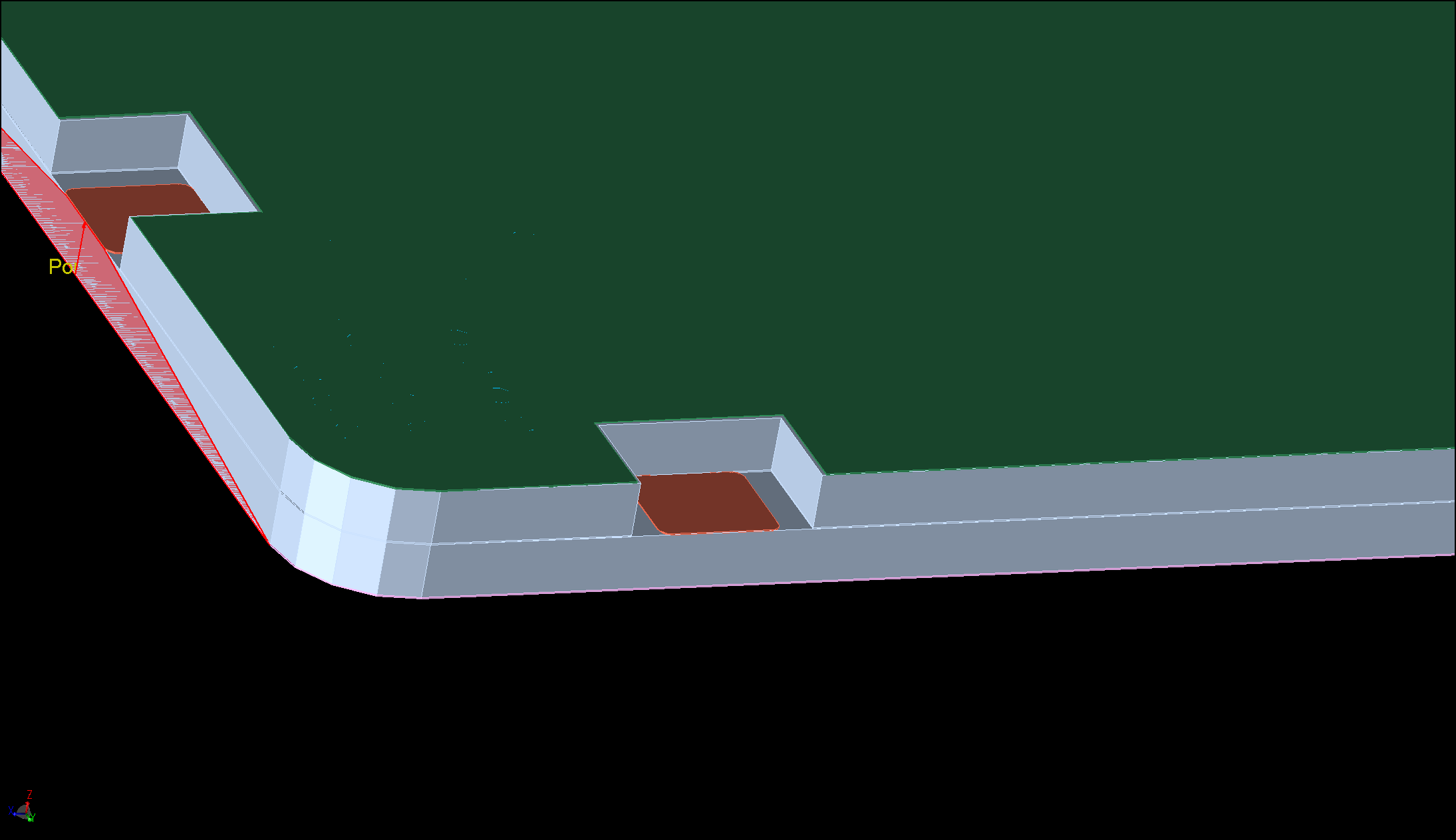
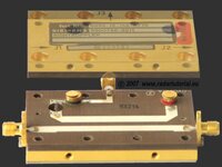
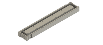
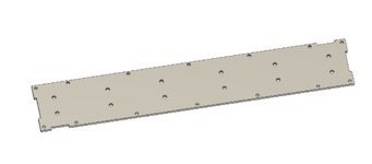
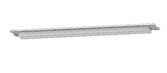
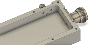
Hi, I have a question about connection to the stripline structure, how it usually done? My board is directional coupler in VHF range, that is made from two laminates + prepreg. I need to connect coaxial connector to the central layer, so in the design I made cutout in the second (top) laminate for the connector pin. I am not sure is it correct or not, but I have bad port to port isolation, which is crucial for a directional coupler. Simulation shows much better parameters.
On pictures how it all look like, connector's pad has width for the microstripline design, other lines width for stripline. Also not sure about board's technical feasibility, prototypes that were made had cutout likewise that made after baking with prepreg.
6.png

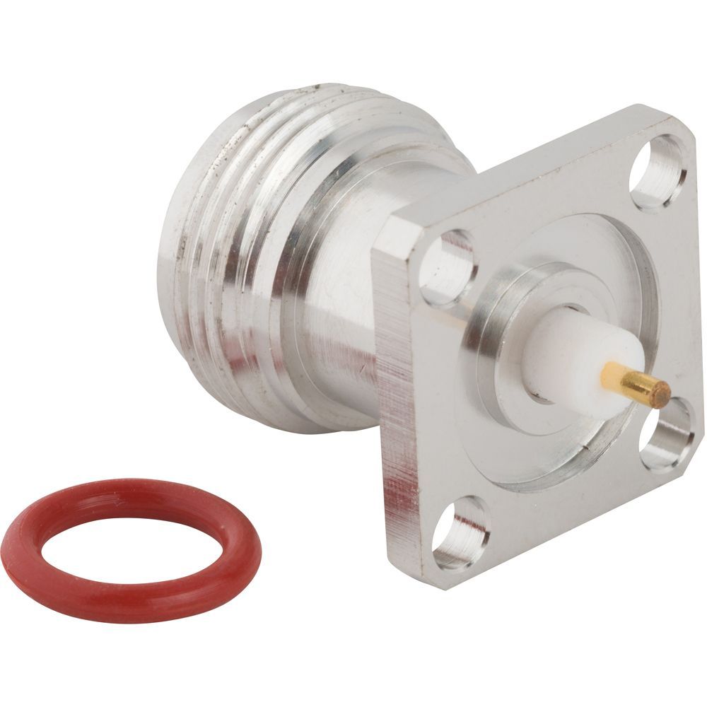
ntype.jpeg

3.png
 
show test results and design assumptions for test & dimensions for W, H, L, PTH, Er, f,
Er reduces with Microstrip as it shares one side with air Er=1 but depends on f whereas Stripline does not share Er with air.
 
Last edited:
A small aperture shouldn't effect too much the response. Either there are manufacturing faults OR simulation errors. Both are also possible.
I would use SMA instead of N-Type connector if there isn't any obligation. Insomuch as, I'd use tip connection featured SMA connector.
They have very small central conductor tip that just touches to the line.
 

D.A.(Tony)Stewart

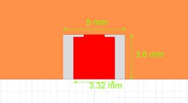
Width for microstrip part 3.32 mm, for stripline 1.636 mm, thickness 60 mil +4 mil prepreg +60 mil Er 3.6. "Window" cut out in top laminate 5 mm width and 3.5 mm length. Main problem is isolation between main line and reflected, port 1 to port 4. It is around 62 dB, but should be 74 dB at least. My concern is "window" and part of the connector with teflon ring.

BigBoss

N type is dictated by high power. Actually I am almost confident that all problems come from connection (chassis-RF connector-board). I've already build similar directional coupler, but 1) used different connector with flat pin and without teflon ring. 2) Did not used prepreg, just clamped two layers together. 3) Did not use stripline-microtrip transition I just kept same width everywhere and grinded by dremel grooves in the top laminate, so flat tab of the connector fitted inside laminate. First board worked well, but wasn't technological, too much complication during assemble.
flat_tab.jpeg

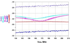
46dB_test.png
 
How did you tie both TOP and BOTTOM layers to the enclosure ?? Do not say to me "with screws".
TOP and BOTTOM layers have to be tightly connected to the enclosure. Also there must be sufficiently much Top-to-Bottom Via and both layer should be tied to the enclosure over many points.
 
Regarding old design without prepreg. There was second aluminum plate on the top, so i tighten (with screws) metal to metal and pcb inside, also rf connectors were tighten to both metal plates so ground were more or less uniform. I thought that "normal" board with pregreg and "nornal" enclosure will work better than DIY, but in reality not.
 
The OD of insulation to OD of center conductor determines the Zo for a given Er.

From the pixels the ratio is 3.4 to 3.5
Beyond that is the compression ring which is more likely to be elastic and not teflon. So that would be purely mechanical. But having it 50% exposed over the microstrip is unusual.

I would be most concerned about the all the conductor interfaces and use gasket for the lid and check torque on connector fasteners.

The 3D to 2D EM model parameters are missing for me to understand where the issue is without a 3D model with all the s plots.

Can you provide more plots on all 4 ports thru and reflected?
 
I have access to only 2 port VNA, so I put all measurements on one graph, but during measurements I switched ports. I've checked my coax loads, cables and they are Ok.
On graphs the only "wrong" parameter is isolation its around 62dB, hence (D) directivity is also poor. Should be 74 dB.
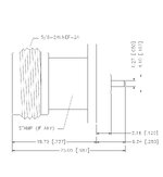
I did not simulated connector in 3D, only board, considered overkill. In datasheet for connector outer diameter 4.1 mm and central conductor 1.27 mm, length of the segment is 3.18 mm, rough calculation with Er 2.1 gives 49 Ohms, in the datasheet it is stated that insulator is teflon/ptfe.

I tried to tighten/loosen screws, measuring without top lid, took off silicon gasket, put copper foil to create addition thickness, none of those have sensible affect. Also I have assembeled two couplers and they have +-0.5% parameters. I simply do not understand how usually connectors connected, here inside spoiler photo of siemens board which is also stripline, but despite being commercial build, it doesn't have prepreg. If look carefully it seen that there is no any stripline-microstrip transition and no cutouts or groves for connector pin.
meas46.jpgcoax_ntype.jpgrk.big.jpg
 

Attachments

  • 172117-30.pdf
    61.3 KB · Views: 35
Can you show a more detailed picture (or photo) of your coax to PCB transition?
Is your directivity poor because the return loss of the trough line is poor?
 
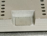
Here is detailed picture of the board. Connector's pin soldered directly on the pad.
Real board has "trapezoidal" shape cut out, don't know is it normal situation or fault of the production I am just not familiar with technology of stripline boards.
port_cut.jpg
IMG_20240218_230048_.jpg
I don't have "time gating" option on vna, therefore I can't clearly say that return loss exactly at port is bad or not, i see only combined s11, s22, and they are good, 35 dB.

For now am setting up router to increase port window from 5 mm to 7 mm.
 
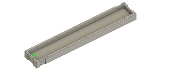
@Altyn1000 Ok, now I finally understand your 3D picture in post #1 with port & cutout configuration.

The overall return loss looks good, then indeed something else is going on. BigBoss asked about connection of your top/bottom grounds to the connector, and you seemed confident that this works well, but what else could degrade your isolation then? Have you tried wrapping a copper sheet around the edge, to connect top and bottom near the connectors?

In #4 you mentioned a version that worked well, but I didn't quite understand which of the three modifications listed there did the trick, and why?

What I could offer to support you is 3D EM of the PCB with connector, if you are willing to provide the design data. ADS workspace would be fine, or DXF + stackup data.
 
Here is detailed picture of the board. Connector's pin soldered directly on the pad.
Real board has "trapezoidal" shape cut out, don't know is it normal situation or fault of the production I am just not familiar with technology of stripline boards.
View attachment 189141
View attachment 189143
how does this show the interface of your board to the N connector conductors and dielectric?
Width for microstrip part 3.32 mm, for stripline 1.636 mm, thickness 60 mil +4 mil prepreg +60 mil Er 3.6. "Window" cut out in top laminate 5 mm width and 3.5 mm length.

Can you not create an accurate plan view and end view drawing?
 
I was curious and simulated the coupler, based on the data that you mentioned above. Gap in my model is 4.1mm, coupled length is 232mm. Top and bottom cover is 2mm thick.

There is no issue with locally removing the top dielectric, that works fine.

Note that in my model, the coax shield has proper connection to top and bottom ground cover, it touches both metals.

Overview:
coax_geom1.jpg


Detail with top cover hidden:
coax_geom_topcover_hidden.jpg


Simulation results, isolated port is port 4 in my model:
coax_result.png
 
Here the essential question is that how the PCB GND is connected to the enclosure and how the connector body is tighten to the closure.
Simulation environment is ideal but how about the practical reality ?
Isolation/Directivity problem says to me that there is a unwanted coupling through/via enclosure even it's opened/closed. Have you ever checked resonance modes of the enclosure ?? It might be small ( just in case )
 

D.A.(Tony)Stewart

Yes that picture pretty correct, and model by volker@muehlhaus also correct.
Note that in my model, the coax shield has proper connection to top and bottom ground cover, it touches both metals.
If am correct on the picture "P1E blue material" is ground metal surrounding coax connector, in my coupler ground path goes 1) connector 2) al6061 enclosure 3) board. I don't know how actually implement assembly where top and bottom will be perfectly symmetrical. In my enclosure thickness of the wall near connectors is 3 mm. Additionally my covering plate do not cover area with pins, I was afraid of possible arc. From pictures there are three parts, first, main enclosure, second, insert that pushes board, and third top lid. When tightened together board's both top and bottom touch metal but "path" for top layer longer. I tried to wrap board with foil, but not exactly above connectors, I will try this.
In #4 you mentioned a version that worked well, but I didn't quite understand which of the three modifications listed there did the trick, and why?
I don't know, but I have connectors that i used in the old prototype, and will try new board with them, hence exclude effect of the enclosure and see if there is difference.
Have you ever checked resonance modes of the enclosure ?
No, I actually do not know how to do it. But I found interesting thing when I remove push in insert (that connects top cover of the board to the enclosure), isolation grows, just from 62 to 64 dB. Also I found that enclosure is not perfectly flat, but when I tighten board touches enclosure everywhere without gaps.

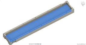
3_.jpg2.png8.png12.png6.pngf1.jpg Board lays on "blue highlighted surface"
 
In my enclosure thickness of the wall near connectors is 3 mm.
The coax dielectric length is 3.18mm, so that there might be a gap between the enclosure side wall and the PCB, and ground current take some extra path length. However, that should also be visible in return loss of the main line.

One other question: have we discussed the coax connections of the coupled line at all? If there is some mismatch at the connectors there, this would show up in directivity. So we should look at these PCB<>connector interfaces as well.
 

LaTeX Commands Quick-Menu:

Part and Inventory Search

Welcome to EDABoard.com

Sponsor

Back
Top