Continue to Site

Welcome to EDAboard.com

Welcome to our site! EDAboard.com is an international Electronics Discussion Forum focused on EDA software, circuits, schematics, books, theory, papers, asic, pld, 8051, DSP, Network, RF, Analog Design, PCB, Service Manuals... and a whole lot more! To participate you need to register. Registration is free. Click here to register now.

Layout review DS90UB960-Q1 interface with SC206E

newbie_hs

Full Member level 1
Joined
Mar 4, 2023
Messages
96
Helped
1
Reputation
2
Reaction score
1
Trophy points
8
Activity points
770
Dear Team,

This is a continuation of this question.
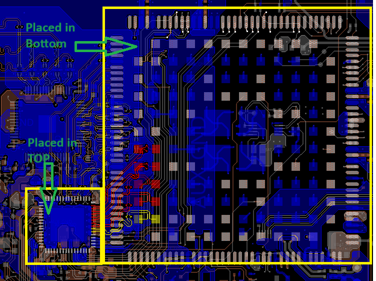
In my board DS90UB960 is placed in top and SC206E is placed in bottom.
Please see the below image
1702889891014.png


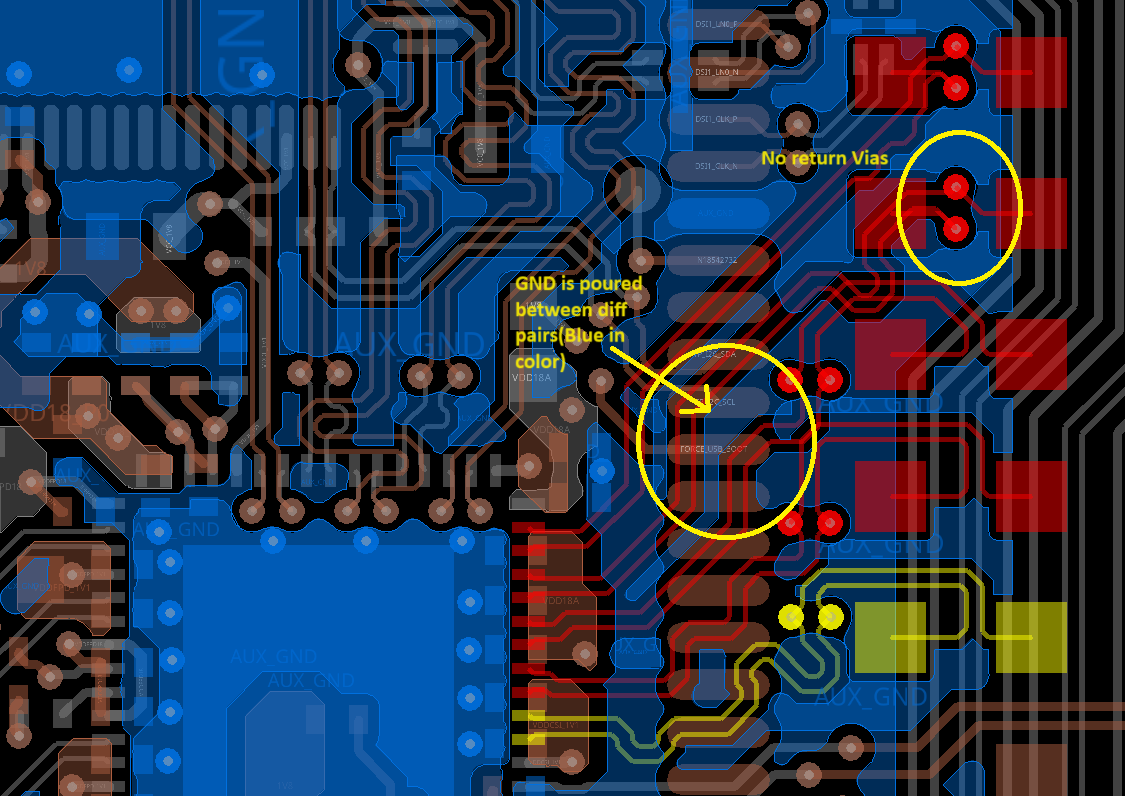
Below is the enlarged version of CSI0 interface. The yellow color signals are clock and red color are CSI0 t0 3 data line.
These signals are travelling from top to bottom. But there is no return vias are provided.What you see in blue color is the ground
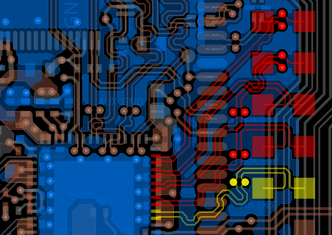
  1. My question is do we need to place return vias near symmetrical to the vias which are moving from top to bottom.
  2. Is it a good idea to pour GND in between differential pairs.You can see that in between CSIO_D1 and CSI0_D2 gnd is poured.As per my knowledge this will affect the impedance of the trace.Please correct me if I am wrong

1702890002621.png

1702890966575.png

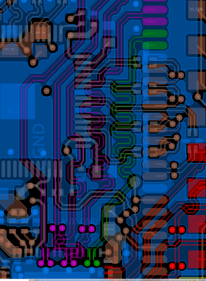
Below is the CSI1 signals. Green is the clock
1702890341896.png


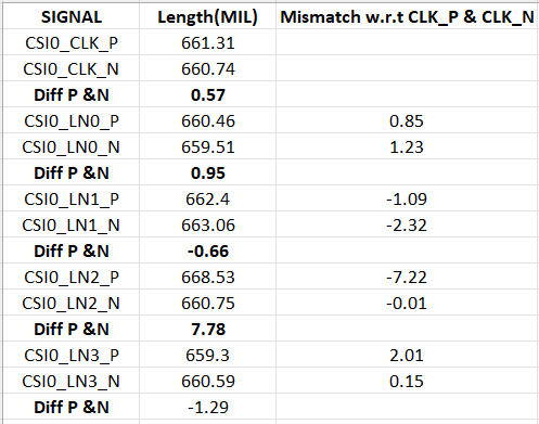
Trace length details are given below.
1702890398993.png
 
Last edited:
Hi,

1) If your differential lines/traces are completely identical in length there will be no GND return current, so there would not be need to think about it. Nevertheless, they are not, so here your return current origin will be a GND (pin) connection of your IC. The question would be where the next GND pins of your ICs are. On first glance it even looks like you are not providing an uninterrupted "direct" GND path/plane between the two ICs next to the differential lines. So your return current will travel somewhere along your PCB (path of lowest impedance). Note, by not providing a constant GND "condition" under and beside your differential lines will have an impact on the impedance as well.

2) yes, that's correct. You may check the b impedance with a design tool e.g. [1]

[1] https://saturnpcb.com/saturn-pcb-toolkit-help-htm/

BR
 
On first glance it even looks like you are not providing an uninterrupted "direct" GND path/plane between the two ICs next to the differential lines
My Deserializer is present in L1 and L2 is complete GND plane SC206E is present on L6 and L5 is complete GND plane.
L3 is VCC+ GND and L4 is VCC
 
Ok, in the attached pictures I only can see the blue (Aux GND?) plane (layer?), and that one seems to be interupted along the clock lines. Unfortunately, I'm not able to attach an image via rhe mobile phone to indicate the region.
 
My Deserializer is present in L1 and L2 is complete GND plane SC206E is present on L6 and L5 is complete GND plane.
L3 is VCC+ GND and L4 is VCC
here I can read: (all just copy and paste without modification):
* My Deserializer is present in L1
* My Deserializer is present in L1 and L2
* L1 and L2 is complete GND plane
* L2 is complete GND plane
* L2 is complete GND plane SC206E
* GND plane SC206E is present on L6
and so on...

Is it so hard to give clear informations? Like:
* L1 = ...
* L2 = ...
* L3 = ...
...

Klaus
 
With respect to the impedance you should aim for constant conitions i.e. trace width, trace to trace spacing, GND below and GND between the traces or no GND at all. Every deviation will lead to a change of the target impedance. In generell I would recommend to keep GND planes between the individual diff-pairs, thlo shield them from each other. Here, spatial seperation is favourable.

Based on the pictures atteched, I miss VIAs to connect the individual GND layers, but I only see a snippet and it may not be feasible to but additional VIAs.

With respect to te return GND path. Check if there is an uninterrupted GND path from IC #1 to IC #2, next)most likely ubder the diff-lines. Here the return current will leave/enter by a GND pin of the ICs.
 
here I can read: (all just copy and paste without modification):
* My Deserializer is present in L1
* My Deserializer is present in L1 and L2
* L1 and L2 is complete GND plane
* L2 is complete GND plane
* L2 is complete GND plane SC206E
* GND plane SC206E is present on L6
and so on...

Is it so hard to give clear informations? Like:
* L1 = ...
* L2 = ...
* L3 = ...
Please see my stackk-up below

L1 : Signal Layer Deserializer is present here.
L2 : GND
L3 : VCC+GND
L4 : VCC
L5: GND
L6: Signal layer SC206E is present in this layer
--- Updated ---

With respect to te return GND path. Check if there is an uninterrupted GND path from IC #1 to IC #2, next)most likely ubder the diff-lines. Here the return current will leave/enter by a GND pin of the ICs.
Differential pairs are moving from L1 to L6.Solid GND planes are present below differential pairs only on L2 and L5
 

LaTeX Commands Quick-Menu:

Part and Inventory Search

Welcome to EDABoard.com

Sponsor

Back
Top