mohamis288
Full Member level 3
Hello,
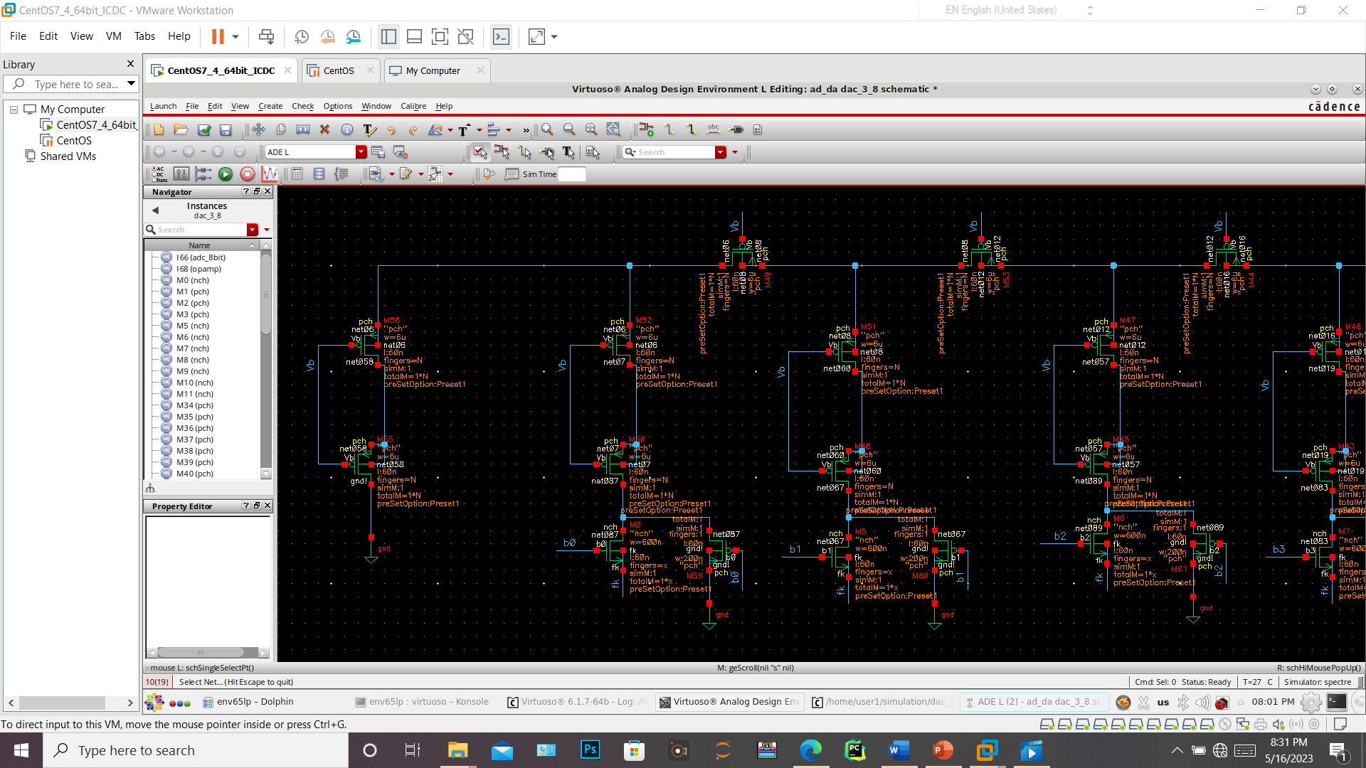
I have designed a circuit like this:

This is a R-2R DAC. lower transistors in each arm, are used to connecting the arm to real ground and virtual ground. those which are connected to virtual ground made up our DAC output. control voltages are outputs of 8-bit ADC and its output voltage is between 1.2 and -1.2 . but cadence gives warning:
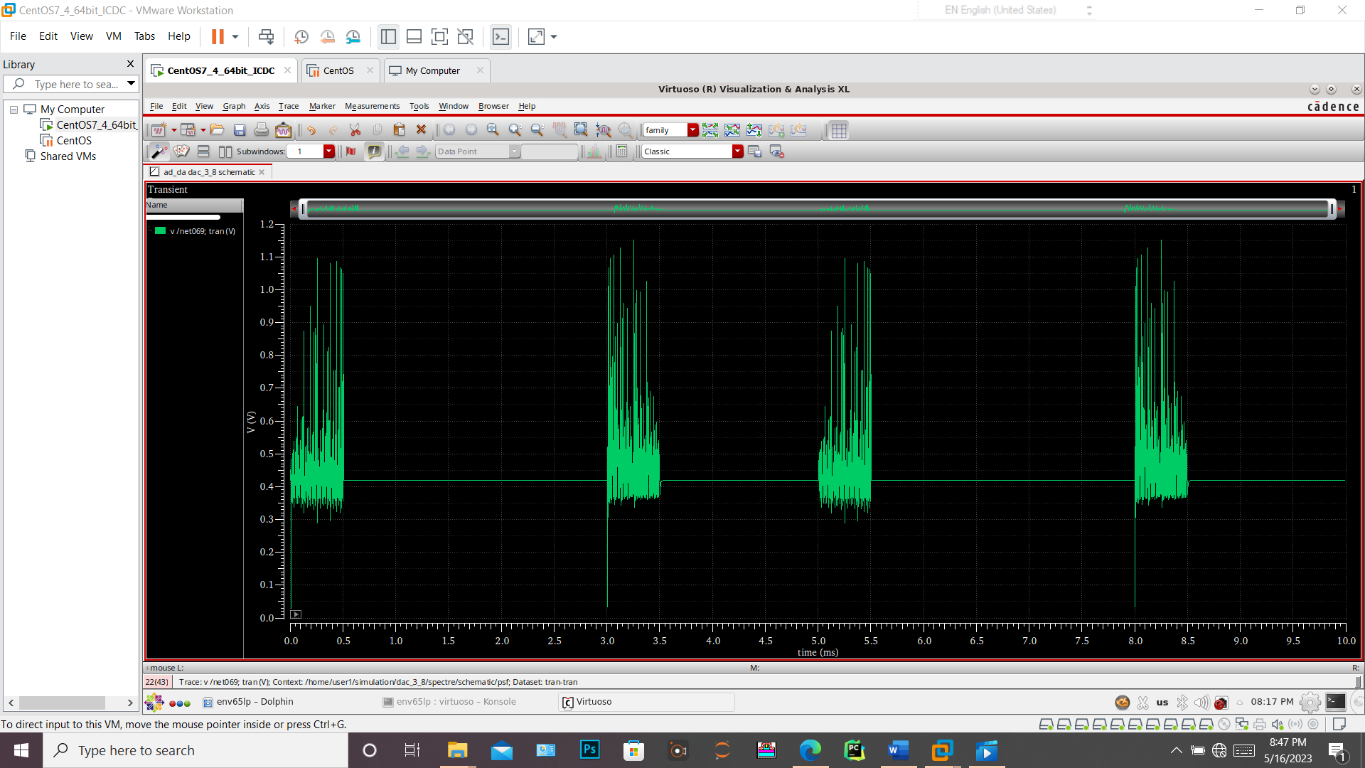
Both clock and input signal to ideal ADC which provides our control voltage are "vpulse" functions. the output would be like this which is not acceptable:

what is the problem?
any help would be appreciated.
I have designed a circuit like this:
This is a R-2R DAC. lower transistors in each arm, are used to connecting the arm to real ground and virtual ground. those which are connected to virtual ground made up our DAC output. control voltages are outputs of 8-bit ADC and its output voltage is between 1.2 and -1.2 . but cadence gives warning:
Code:
Warning from spectre at time = 250.502 us during transient analysis `tran'.
    WARNING (CMI-2682): M0: The bulk-drain junction forward bias voltage (797.149 mV) exceeds `VjdmFwd' = 793.148 mV.  The results are now incorrect because the junction current model has been linearized
Warning from spectre at time = 250.502 us during transient analysis `tran'.
    WARNING (CMI-2682): M5: The bulk-drain junction forward bias voltage (794.799 mV) exceeds `VjdmFwd' = 793.148 mV.  The results are now incorrect because the junction current model has been linearized
Warning from spectre at time = 250.502 us during transient analysis `tran'.
    WARNING (CMI-2682): M6: The bulk-drain junction forward bias voltage (793.641 mV) exceeds `VjdmFwd' = 793.148 mV.  The results are now incorrect because the junction current model has been linearized
Notice from spectre at time = 250.502 us during transient analysis `tran'.
    M6: The bulk-drain junction returns to normal bias condition
Notice from spectre at time = 250.502 us during transient analysis `tran'.
    M5: The bulk-drain junction returns to normal bias condition
Notice from spectre at time = 250.502 us during transient analysis `tran'.
    M0: The bulk-drain junction returns to normal bias condition
Warning from spectre at time = 375.502 us during transient analysis `tran'.
    WARNING (CMI-2682): M0: The bulk-drain junction forward bias voltage (798.932 mV) exceeds `VjdmFwd' = 793.148 mV.  The results are now incorrect because the junction current model has been linearized
Warning from spectre at time = 375.502 us during transient analysis `tran'.
    WARNING (CMI-2682): M5: The bulk-drain junction forward bias voltage (794.957 mV) exceeds `VjdmFwd' = 793.148 mV.  The results are now incorrect because the junction current model has been linearized
        Further occurrences of this warning will be suppressed.
Notice from spectre at time = 375.502 us during transient analysis `tran'.
    M5: The bulk-drain junction returns to normal bias condition
Notice from spectre at time = 375.502 us during transient analysis `tran'.
    M0: The bulk-drain junction returns to normal bias condition
        Further occurrences of this notice will be suppressed.
Both clock and input signal to ideal ADC which provides our control voltage are "vpulse" functions. the output would be like this which is not acceptable:
what is the problem?
any help would be appreciated.