Continue to Site

Welcome to EDAboard.com

Welcome to our site! EDAboard.com is an international Electronics Discussion Forum focused on EDA software, circuits, schematics, books, theory, papers, asic, pld, 8051, DSP, Network, RF, Analog Design, PCB, Service Manuals... and a whole lot more! To participate you need to register. Registration is free. Click here to register now.

How to design high power RF trace on thin PCB RF-4 to meet 50 Ohm trace impedance?

Status
Not open for further replies.

coolpixs4

Junior Member level 2
Joined
Jun 4, 2010
Messages
20
Helped
0
Reputation
0
Reaction score
0
Trophy points
1,281
Location
Korea
Activity points
1,437
I need to design a microstrip power splitter for high power RF signal of about 40dBm (10W)
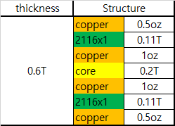
on a PCB of FR-4 (Er=4.5) with 4-layers( 0.5oz/0.11T/1oz/0.2T/1oz.0.11T/0.5oz)
1657692061627.png


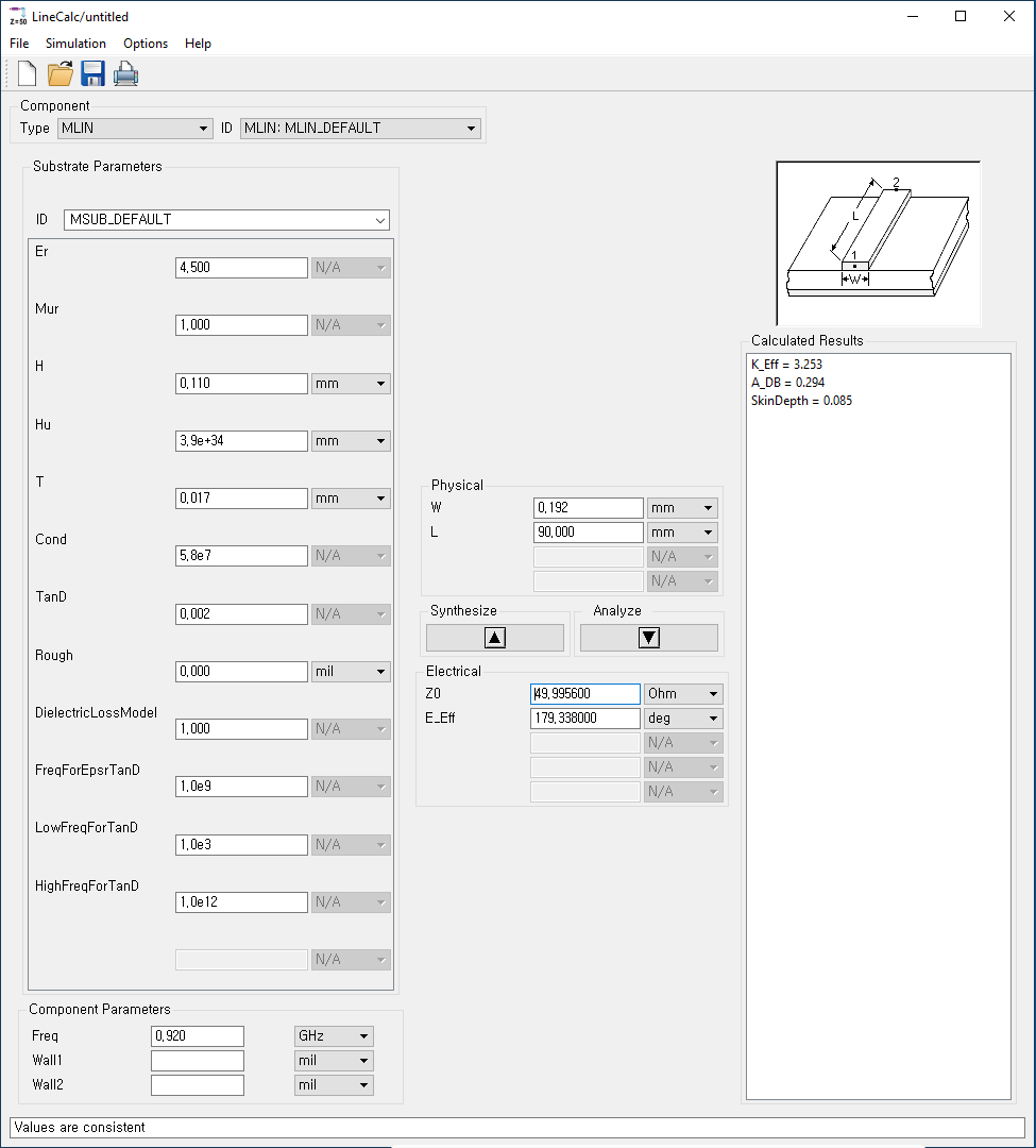
So, by using ADS-LineCal tool, the calculated 50-ohm trace impedance results in a very small width of the trace 0.192mm
1657692251026.png


I thought this trace width line cannot carry the signal of 10W, a lot of heat will burn the trace
If increasing the trace width up to 1.1mm or higher value => without the change of total substrate height

Is it possible to design a power microstrip splitter on that substarte ?

Thanks
 
Last edited by a moderator:

Not the best substrate to use, but it will work. Try increasing the distance between layers, i.e top track signal and bottom ground. Don't use the inner layers, that will give you a thicker track width for 50 ohms.
 

Not the best substrate to use, but it will work. Try increasing the distance between layers, i.e top track signal and bottom ground. Don't use the inner layers, that will give you a thicker track width for 50 ohms.
Thanks for your comment.
But the substrate structure cannot be changed due to relating to other parts of other works, they just request me to re-design a microstrip power splitter for a 10W RF signal (each branch) to two antenna ports
the trace at each end port must use the width of 1.1mm (for ~1.15A current) - this means each end line impedance of about 15-ohm can not be match to 50-ohm ports

The previous person's design seems not correct to matching 50-Ohm.
so S11, S22 = -2db
S21 = -6.8db ( 1 port open)
S21= -9dB ( if 1 port terminated by 50-Ohm term)
1657756886986.png

What should I do, does use LC matching circuit can improve this ?
 

You seem to be severely constrained as to what you can do.
The 1.1A current rating is for DC, at RF you have to account for skin effect this makes the loss higher than the resistive loss.
I do not know why the main transmission lines are 25 ohm impedance, if this was transform each 50 ohm to 100 ohm at the junction then the lines should have been 70 ohm.
Even if you use LC matching you have to get the signal to the circulator output., but it may be helpful to get to a useful intermediate impedance.
If the transmission line connecting to the circulator is 50 ohm then the other lies are higher impedance not lower.
At 900MHz you do need to keep the impedances under control, even short length acts as a transformer and needs to be accounted for.
Your best bet may well be to use what ever track widths you can, within reason the thicker the better and see what impedance you get at the junction. A thicker line will move the transformed impedance at the junction further from 100 ohms making the final match more difficult.
Then use LC matching to match the two antenna lines to the circulator. Don't forget to account for the line length to the circulator. You will also have to use components able to handle the power, high quality capacitors and inductors.
Don't expect the match to be good if only one port is terminated, the circuit you show relies on both ports having terminations.
If three is no circuitry under the splitter and no other tracks, it would make things much easier if you just have two layers; top and bottom.
 

Status
Not open for further replies.

Part and Inventory Search

Welcome to EDABoard.com

Sponsor

Back
Top