Continue to Site

Welcome to EDAboard.com

Welcome to our site! EDAboard.com is an international Electronics Discussion Forum focused on EDA software, circuits, schematics, books, theory, papers, asic, pld, 8051, DSP, Network, RF, Analog Design, PCB, Service Manuals... and a whole lot more! To participate you need to register. Registration is free. Click here to register now.

how a RF connector being connected onto complex RF PCB

yefj

Advanced Member level 4
Joined
Sep 12, 2019
Messages
1,193
Helped
1
Reputation
2
Reaction score
3
Trophy points
38
Activity points
7,205
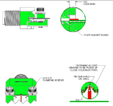
Hello, i need to use the follwing connector for the pcb stackup shown below.
I know that the middle layer is the ground for RF.
How does such connector works with the PCB?
How does this connector connects to the midl layer as its ground and top layer as signal?

1704997409413.png

1704997360149.png
 
Datasheet shows expected ground conductors on PCB top and bottom. They'll be connected to inner ground plane with multiple vias.

1000003329.jpg
 
Using a very toxic BeCu (Beryllium Copper) as a launch pin, would make me to think twice to use this connector.
Connector, which anyway, I don't think a normal RF circuit design worth its complexity. Unless will be part of a Moon or Mars travel project.

 
is there a practical manual on how i need physicly mount it on the PCB?
Thanks.
 
Using a very toxic BeCu (Beryllium Copper) as a launch pin, would make me to think twice to use this connector.
Connector, which anyway, I don't think a normal RF circuit design worth its complexity. Unless will be part of a Moon or Mars travel project.

Just a tad over-reaction. It's gold plated BeCu, I believe for spring properties and precision at 35 GHz.
 
Hello , could you please point to the part where we connect to the RF ground plane?
the ground plane at my PCB is in the middle so i am i cant see where do we connect our middle gnd RF layer to the connector?
Thanks.
1705163180501.png
 
Hello FVM, i am having trouble to imagine it.
maybe the side screws needs to touch the ground pane ? why on the other layers i need to put a VOID so these screw wont touch them?
Thanks.
 
Like any end-feed SMA the pin connects on the top layer. But this 50 to 100 GHz version creates a large keep out area on the top layer of copper near the signal going out in small fan to avoid surface roughness and relies on the bottom side ground plane to maintain impedance for these millimeter wavelengths. The pin must be berryllium to have the spring properties with tension when clamped.

Solder would screw up the return loss. Don't screw it up either in your layout.

So we may assume that you are planning to use to the 8 GHz YIG Osc. to multiply up with another VCO into this frequency range using another PLL with a prescaler to mix down.


Red = Signal,, Green = slime

1705190884038.png


In order to have a 50 Ohm line as thin as shown in their test coupon board means the substrate to gnd layer must be very thin and/or high (10) Dk like Alumina.
But different models exist for various thickness boards.

ETA of working system 2030
 

Attachments

  • 1705177296242.png
    1705177296242.png
    118.9 KB · Views: 36
Last edited:

LaTeX Commands Quick-Menu:

Part and Inventory Search

Welcome to EDABoard.com

Sponsor

Back
Top