Continue to Site

Welcome to EDAboard.com

Welcome to our site! EDAboard.com is an international Electronics Discussion Forum focused on EDA software, circuits, schematics, books, theory, papers, asic, pld, 8051, DSP, Network, RF, Analog Design, PCB, Service Manuals... and a whole lot more! To participate you need to register. Registration is free. Click here to register now.

trace thickness of RF amplifier question

yefj

Advanced Member level 4
Joined
Sep 12, 2019
Messages
1,192
Helped
1
Reputation
2
Reaction score
3
Trophy points
38
Activity points
7,199
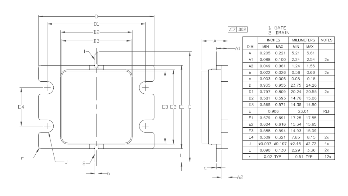
Hello, given the datasheet shown below.
I cant understand what is the thickness of the trace.
generally its in units of Oz.What dimention should i use for this case.
Thanks.
1708856133474.png
 
Hi,

what thickness of which trace?

Thickness has only minor influence on impedance / characteristic impedance.

But for if you are talking about high current you need low ohmic resistance to reduce power dissipation = heat.

Btw: trace thickness = copper thickness in non US often is given in micrometers. 1OZ copper per square inch equals to about 35um copper thickness.

Klaus
 
Due to skin depth of few um at microwave frequencies, copper weight matters only for DC current. You should know if it's critical for your design. Standard copper weight is 1 oz also for microwave substrates, I would use it in case of doubt.
 
Case is mounted directly to the heat sink, not to the PCB, so PCB copper thickness has very little effect on thermal design for this application.
 
1 oz copper is a weight density measured in ounces per square foot (oz/(ft^2).
Using the density of copper which is 8.96 g/cm^3, we can calculate the thickness of 1 oz copper = 1.4 mils = 34 μm (microns) thick.
 
Drain current
You are right, but forgot to mention the 10% duty cycle mentioned in the data sheet. From what I understand, we have 3A effective worst case. If we assume 1.2mm trace width at 1oz (35micron) thickness, trace temperature rise would be less than 15K.
 
@volker@muehlhaus I hope @yefj understands this datasheet does not specify any results for > 10% DC or Vds< 45V or CW operation.

There is also an exotic substrate with tapped holes for the fasteners and solder filled thermal vias to the PCB heatsink interface
This would be a significant challenge to reflow solder or wave solder onto a heatsink so I suspect it is all done with a Metcal iron by hand.

The edge-mount SMA's have tapped fasteners.
PTFE over Al-SiO2 or core–shell structured hexagonal boron nitride coated hollow glass microsphere are my guesses.

I might considering using ceramic over sponge copper substrate H2O cooled for pulsed 500W.

The Eval PCB must be better than the RθJC= 0.42°C/W which is not stated, for either mat'l type, Rth, thickness or additional cooling.

For 50 Ohms from the trace width that the substrate must be 1/3 to 1/2 of the trace width depending on Dk.

Notice the thickness of the looped (est.) 30 nH DC power jumper compared with the thickness of the signal feed width for thermal and electrical resistance.

The ears over the RF pins out of the ceramic package must be custom made on this Eval board to provide the necessary gap for 50 Ohms around the pin.

1708976220205.png
 
Last edited:

LaTeX Commands Quick-Menu:

Part and Inventory Search

Welcome to EDABoard.com

Sponsor

Back
Top