Continue to Site

Welcome to EDAboard.com

Welcome to our site! EDAboard.com is an international Electronics Discussion Forum focused on EDA software, circuits, schematics, books, theory, papers, asic, pld, 8051, DSP, Network, RF, Analog Design, PCB, Service Manuals... and a whole lot more! To participate you need to register. Registration is free. Click here to register now.

how to design a Fly-back converter for switching power supply.

Status
Not open for further replies.

Raees

Junior Member level 2
Joined
Jun 6, 2013
Messages
23
Helped
0
Reputation
0
Reaction score
0
Trophy points
1,281
Activity points
1,471
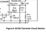
Hi everyone. I want to make a transformer myself. I using the following application note

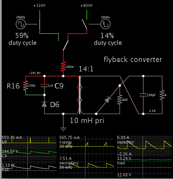
my input voltage is similar that is in this application note, that is 130VDC to 800VDC.
output voltage = 12VDC 2Amp.

i tried to make myself by using the calculation, and it is working too but the problem i m facing is in snubber circuit. i have used 300 ohms and 20 Watts and they are heating like hell. i m sure there is leakage inductance. but how to reduce it? any one plz help.
 

Attachments

  • Fly back Converter 850Vin-12Vout 0.75A Circuit notes.pdf
    321.6 KB · Views: 106

i tried to make myself by using the calculation, and it is working too but the problem i m facing is in snubber circuit. i have used 300 ohms and 20 Watts and they are heating like hell.
This is somehow different from the reference design. You are talking about the same RCD snubber topolgy? How did you arrive at this nearly absurd value? Which leak inductance related primary overvoltage do you admit?
 

Thanks FvM for the response.

Here in Pakistan, not every desired component is available. There i m using MOSFET "IRFBG30" in place of MTB.... both have almost similar operating characteristics but different input to output capacitance. There i just tried hit-and-trial method to get better waveform at Mosfet's Drain.

This is the waveform at default snubber components.
**broken link removed**

This is the waveform at my replaced snubber-components.
R(R16)=3 X 100ohm (20W); Cap(C9)= 68Pf 3KV //68Pf 3KV//68Pf 3KV
I have also replaced MUR1100E by BYW51200 because at the time of trial when input increased upto 400V, this diode including primary winding burned. i thought that the Ampere rating is below. therefore i tried to replace with a higher rating. But circuit topology is same.
**broken link removed**
 

A RCD snubber has the purpose to limit the transistor peak voltage. There may be still oscillations after commutation of the snubber diode.

The RCD dimensioning rules are
- select C so that it limits the peak voltage to a safe level
- select R to allow C to discharge at least partly before the next pulse, e.g. RC ≈ PWM-period.

Your low R value effectively contradicts the RCD operation principle. To damp oscillations, you can try with an (addional) RC series snubber.

Flyback converters for high input voltage are a bit problematic. It may be better to go for a two-switch forward or flyback topology that has built-in clamping of leakage inductance overvoltage.
 

    V

    Points: 2
    Helpful Answer Positive Rating
Looking at the schematic, R16 (in snubbing network) shows a value of 100k ohms.

You state your R16 value as 300 ohms.

Even at 100k, this resistor must dissipate 1W of heat. The reason is that the transformer generates -190V during switch-Off period (according to my simulation).

Your 300 ohm resistor carries about 60W avg.


    V

    Points: 2
    Helpful Answer Positive Rating
Dear Bradthered, U have applied 20 KHz frequency on both input voltages while in the document and in my circuit too, its working on 70KHz to 140KHz variable frequency. secondly your primary inductance is different than in document. so do these changes values put some effects on your observations?
 

Dear Bradthered, U have applied 20 KHz frequency on both input voltages while in the document and in my circuit too, its working on 70KHz to 140KHz variable frequency. secondly your primary inductance is different than in document. so do these changes values put some effects on your observations?

I revised my simulation using your values. I adjusted the transformer primary to 2 mH.

The snubber action changes little. The coil still has 800V, alternating with 200V (give or take).

A 100k value for R16 dissipates 880 mW.
 

In the pdf the OP posted in his first post, on page 7 of 12 there is a schematic. On the bottom of R13 and R14 there is a semi circle drawn. Does anyone know what that means.
 

Attachments

  • semi circle.JPG
    semi circle.JPG
    42.8 KB · Views: 88

In the pdf the OP posted in his first post, on page 7 of 12 there is a schematic. On the bottom of R13 and R14 there is a semi circle drawn. Does anyone know what that means.

It is connected with the Input-Ground.
 

Status
Not open for further replies.

Similar threads

Part and Inventory Search

Welcome to EDABoard.com

Sponsor

Back
Top