Continue to Site

Welcome to EDAboard.com

Welcome to our site! EDAboard.com is an international Electronics Discussion Forum focused on EDA software, circuits, schematics, books, theory, papers, asic, pld, 8051, DSP, Network, RF, Analog Design, PCB, Service Manuals... and a whole lot more! To participate you need to register. Registration is free. Click here to register now.

Holes error in PDF output of pcb

Status
Not open for further replies.

venkates2218

Full Member level 6
Joined
Sep 30, 2016
Messages
354
Helped
1
Reputation
2
Reaction score
1
Trophy points
1,298
Activity points
4,306
Hai friends i'm designing an pcb using Designspark PCB software...
I need O/P in PDF file..everything working fine but when holes is kept as like in picture i can't get holes on PDF file..

If i reduced the holes size below 6 means i can see the holes in PDF..
Everything in mm unit.... pcb design.jpg
 

Because holes is stored in drill layer. In conductors layers holes never present.
 

Because holes is stored in drill layer. In conductors layers holes never present.


If i changed the holes values to smaller value then holes size shown in picture means i can see the holes in PDF file...
 

Check properly. Holes will be in drill layer. When you want PDF of bottom layer then also check drill layer and get the PDF.
 

i think you are changing PAD diameter not the DRILL diameter and when PAD < DRILL it appears on PDF! i recommend you do a double check.

Ciao!
 

Some PCB tools have a feature to generate copper pads with hole for DIY PCB making. If so, it should be described it manual.
 

DS-screenshot.png

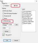
I think you are not creating the PDF correctly. Use following method:
1) Click File > Print
2) Select PDF as shown in the attached image
3) Select the desired layer. You will have to create one PDF for top copper layer and one for bottom copper layer, seperately. Say, you only want TOP layer first. Select TOP Electrical as shown in the image
4) Tick mark All colors black
5) Now this is Important: Uncheck Fill Drill Holes

Click OK to save the PDF.

Hope this solves your issue.
 

I am also facing same problem to convert pcb file to pdf. I use designspark for fabricating my own pcb. But when I convert to pdf, the size differs from actual. I could not overcome this problem.
 

I am also facing same problem to convert pcb file to pdf. I use designspark for fabricating my own pcb. But when I convert to pdf, the size differs from actual. I could not overcome this problem.

Additionally, note that when you print the PDF using laser/inkjet printer, it should be printed without any scaling or shrinking applied.

Uncheck for the pad filling option in your PCB designer software.

Also, many times you feel holes are smaller, but they are not :) ... Smaller holes are OK than the bigger ones. When you do the drilling excess copper will anyways get drilled. But if the hole is bigger, there will be a problem of discontinuity if drill bit diameter is smaller than the hole.
 

I am also facing same problem to convert pcb file to pdf. I use designspark for fabricating my own pcb. But when I convert to pdf, the size differs from actual. I could not overcome this problem.

while printing the PDF file in "SIZE SECTION" choose actual size option...
You can get original scale as your pcb
 

Status
Not open for further replies.

Part and Inventory Search

Welcome to EDABoard.com

Sponsor

Back
Top