Continue to Site

Welcome to EDAboard.com

Welcome to our site! EDAboard.com is an international Electronics Discussion Forum focused on EDA software, circuits, schematics, books, theory, papers, asic, pld, 8051, DSP, Network, RF, Analog Design, PCB, Service Manuals... and a whole lot more! To participate you need to register. Registration is free. Click here to register now.

Fault analysis for CMOS Fabrication

Status
Not open for further replies.

020170

Full Member level 4
Joined
Jan 31, 2005
Messages
231
Helped
3
Reputation
6
Reaction score
1
Trophy points
1,298
Activity points
2,221
Hello.

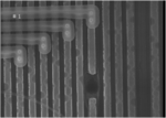
During Fabrication Fault Analysis, I found metal short or open issue.

??1.png

this picture shows top metal lines short.
??2.png

This picture shows metal line open

In my opinion, it looks fabrication issue. because metal line's width is 0.8um, and space is not minimum.

max current is 110uA through opened metal line. current value is not large, current density issue can not be happened.

How about your opinion these issues?

thanks
 
Last edited:

The top metal shorts could have been created by the cross-section grinding.

The metal line open could be over-current (ESD ?) ... or fab issue (dust). Always at the same position?
 

The same-position question is key to resolving whether
these are random litho, or on-mask defects.

I can't see why those "stringers" would be where they
are and so consistently, in fabrication. Normally an
etch failure would leave residual metal at the bottom,
not halfway up. Is there a multi-step interlevel dielectric
involved, or is flat-field ILD thickness half of the metal
height? What does anything like SIMS say about
composition of this "feature"?
 

Status
Not open for further replies.

Part and Inventory Search

Welcome to EDABoard.com

Sponsor

Back
Top