Continue to Site

Welcome to EDAboard.com

Welcome to our site! EDAboard.com is an international Electronics Discussion Forum focused on EDA software, circuits, schematics, books, theory, papers, asic, pld, 8051, DSP, Network, RF, Analog Design, PCB, Service Manuals... and a whole lot more! To participate you need to register. Registration is free. Click here to register now.

error in sample hold circuit.who can help me !

Status
Not open for further replies.

sj_helen

Newbie level 6
Joined
Jun 24, 2006
Messages
14
Helped
0
Reputation
0
Reaction score
0
Trophy points
1,281
Activity points
1,431
who can help me solve this sample hold circuit design problem???

15q50k8.jpg


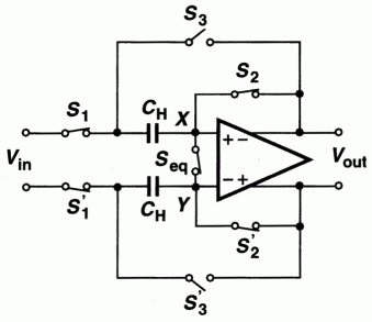
ctrl1 for Sample Phase, ctrl2 for Hold Phase

I designed a opamp, which is used in the basic Sampel&Hold circuit.

The circuit will finish the sample and hold function by switching capacitors.
There are only 2 capacitors in the SH circuits. They are the two differential Sampling Capacitors which are connected to the differential inputs of opamp respectively.

In the Sample Phase, opamp's inputs are shorted and connected to Vcm. opamp's outputs are also shorted, but not connected to Vcm. Two capacitors are sampling differential input signals respectively.

In the Hold Phase, opamp's inputs and outputs are open circuits. Then the "signal" sides of capacitors are connected to opamp's outputs at the same side.

Theoretically, in the Hold Phase, opamp's inputs should be "Virtual Ground" with voltage value equals to Vcm. and the voltages at the differential outputs should be exactly the same as differential inputs.

Now comes two problems:
1,In the Hold Phase, voltage value of opamp's inputs are not Vcm, and a little higher than Vcm.
So how does this happened? and how to deal with this problem?

2,After Sampling and Hold for the first signal, when in the Sample Phase for the second signal, the opamp's outputs should be shorted and the voltage value should be Vcm.
However, simulation results did not prove this. The simulation shows if the already finished first signal is at the highest input signal level, then in the second Sample Phase, ouput voltage level is higher than Vcm; Whereas, if the finnished first siganl at the lowest value, the output level is lower than Vcm.
how does this happened? and how to deal with this problem?

Thanks a lot.
 

04 Sep 2008 20:21 Re: error in sample hold circuit
It would be very helpful (and much more easier to answer) if you could provide a circuit diagram.
Regards LvW
 

A plausible differential S/H circuit is shown e. g. in Razavi, Design of CMOS Integrated Circuits, Figure 12.34. The present circuits seems to be rather an artefact. For instance, an OP wouldn't need (and shouldn't have) a short switch across it's output.

7_1220565783.gif
 

    sj_helen

    Points: 2
    Helpful Answer Positive Rating
FvM's circuit makes more sense to me, but what you are seeing might be due to clock feedthrough. Increasing the capacitor value would help.
 

    sj_helen

    Points: 2
    Helpful Answer Positive Rating
FvM shows a lose loop S/H circuit. sj_helen describes an open loop S/H circuit.

"1,In the Hold Phase, voltage value of opamp's inputs are not Vcm, and a little higher than Vcm.
So how does this happened? and how to deal with this problem? "
Yes, the op,s voltage is not VCM, it relate to the input signal common mode voltage in this unit S/H circuit as your shows. you should calculate the input of op's common mode voltage.

Q2: The op's output common mode voltage should equate the common mode feed back's ref voltage, check you CMFB cirucit.
 

FvM said:
A plausible differential S/H circuit is shown e. g. in Razavi, Design of CMOS Integrated Circuits, Figure 12.34. The present circuits seems to be rather an artefact. For instance, an OP wouldn't need (and shouldn't have) a short switch across it's output.

7_1220565783.gif

Hi, FvM. Thanks for your help. I have checked Razavi's book and saw the S/H circuit you mentioned. The S/H cirtuit I used is from a paper named ''A 1.0V 40mW 10b 100MS/s Pipeline ADC in 90nm CMOS'', with author Hirotomo Ishii, Ken Tanabe, Tetsuya Iida.

I know the principle of the one from Razavi is correct, but I think, since these Japanese guys had already used this S/H circuit in their pipeline ADC, this S/H circuit should work correctly.

FvM, do you see this structure for S/H before? or someone else give comments about its correctness?

Added after 35 minutes:

ytliang said:
FvM's circuit makes more sense to me, but what you are seeing might be due to clock feedthrough. Increasing the capacitor value would help.

Thanks for your help.
but the switch I used now in simulation is ideal switches, so i think clock feedthrough may be not the reason here. Is that right?
 

I doubt, that it can operate as shown. As said, the output short seems dubious to me, also the OP output to signal input short by Ctrl2. It may be understandable from the original publication. Generally, I'm not engaged with IC design, I have Razavi's book as basic literature in my bookshelf, thus I'm not the right guy to suggest a particular solution.
 

jerryzhao said:
FvM shows a lose loop S/H circuit. sj_helen describes an open loop S/H circuit.

"1,In the Hold Phase, voltage value of opamp's inputs are not Vcm, and a little higher than Vcm.
So how does this happened? and how to deal with this problem? "
Yes, the op,s voltage is not VCM, it relate to the input signal common mode voltage in this unit S/H circuit as your shows. you should calculate the input of op's common mode voltage.

Q2: The op's output common mode voltage should equate the common mode feed back's ref voltage, check you CMFB cirucit.

Hi, jerryzhao. Thanks for help.
Yes. I set the common mode voltage of differential input signal exactly equals to the Vcm of opamp, we say for example Vcm=0.45V, Vinp=0.45+0.25, Vinn=0.45-0.25.

The CMFB I use now is also kinda ideal one. Two huge resistors(1G ohms) sense the common voltage of differential outputs, and compare it with the ref voltage, Vcm, then use a voltage-control-voltage source to adjuest the feedback voltage.

Added after 12 minutes:

FvM said:
I doubt, that it can operate as shown. As said, the output short seems dubious to me, also the OP output to signal input short by Ctrl2. It may be understandable from the original publication. Generally, I'm not engaged with IC design, I have Razavi's book as basic literature in my bookshelf, thus I'm not the right guy to suggest a particular solution.

The plot has some mistake, I have corrected it.
OP output is not shorted to signal input by Ctrl2, cause ctrl1 disconnects the capacitor with signal input when ctrl2 is high.
But thanks all the same to give suggestiong about Razavi's structure :)
 

FvM said:
A plausible differential S/H circuit is shown e. g. in Razavi, Design of CMOS Integrated Circuits, Figure 12.34. The present circuits seems to be rather an artefact. For instance, an OP wouldn't need (and shouldn't have) a short switch across it's output.

7_1220565783.gif

This diagram is not correct. But Razavi's book is still the best.
 

To jnuhope:

what's wrong with this closed loop sampling topology from Razavi's book?

I can't figure it out.
 

kennyg said:
To jnuhope:

what's wrong with this closed loop sampling topology from Razavi's book?

I can't figure it out.

Sorry! The fig.12.34 is CORRECT. The fig.12.46 is not correct.
 

Status
Not open for further replies.

Part and Inventory Search

Welcome to EDABoard.com

Sponsor

Back
Top