Continue to Site

Welcome to EDAboard.com

Welcome to our site! EDAboard.com is an international Electronics Discussion Forum focused on EDA software, circuits, schematics, books, theory, papers, asic, pld, 8051, DSP, Network, RF, Analog Design, PCB, Service Manuals... and a whole lot more! To participate you need to register. Registration is free. Click here to register now.

[SOLVED] Em of an inductor with a return path in sonnet cadence

Status
Not open for further replies.

omarelmorsy

Junior Member level 1
Joined
May 9, 2022
Messages
17
Helped
0
Reputation
0
Reaction score
0
Trophy points
1
Activity points
145
hello,
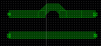
I have created an inductor on metal 9 and a ground plane (return path) on metal 3 as in image1.
The inductor value is intended to be around 80pf, and the inductance value turns to be what I intended, however the quality factor of the inductor is so small around ( 5 ).
the ports used are +-1 and +-2 boxwall ports.

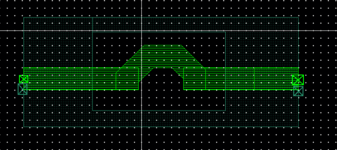
However when I used the return path as a ground rail as in image 2 the quality factor jumps up to 30.

I think there might be a problem with the eming process.
I know that having ground planes for the RF circuits are better than ground rails for less overall noise and better grounding, however this gives me worse quality factor for my inductors.

note: image 1 that is containing ground plane is a part (cut out) from a bigger circuit.
 

Attachments

  • image 2.PNG
    image 2.PNG
    6.8 KB · Views: 118
  • image1.PNG
    image1.PNG
    10.4 KB · Views: 125

Your EM configuration looks ok.

Q factor depends on the loss in signal and return path. What is the resistance (ohm/square) of metal9 and metal3? I assume they are very different?
 
yes, metal 3 has much larger sheet resistance, however my problem here is if I have a large circuit with large ground plane (large width) it would give smaller overall resistance, however the way I cut the circuit (inductor and small part of the ground plane surrounding it ) gives large resistance for the return path, so is there another way to model the overall resistance of the whole ground plane ?
 

and one more thing, isn't the the ground plane insures that it would be the return path rather than the ground rail that may be little far at some circuit parts leading to have another return path than would should actually be ?
 

if I have a large circuit with large ground plane (large width) it would give smaller overall resistance
That's only partially true, because skin effect pushes return current to the edges around the cutout. You can test that by adding larger ground to your Sonnet model, I'm pretty sure that will not help much.

What you could do is to add another metal level in parallel, i.e. stacked metal for return path around the cutout. But that of course applies to the entire path there, it doesn't make sense to apply metal stacking around the inductor only if there is much more metal3 series resistance elsewhere in the path.

There is no easy answer, but you have Sonnet in your hands which can be used to test alternative layout configurations.

Just in general, I would avoid such a symmetric cutout return path, and replace it by a non-symmetric return path where the return current around the slots adds to your indutance (-> direction of current flow). Having symmetric cutout allows return current on one side (here: top/North) that cancels magnetic fields -> reduces industance. So I would push the return metal further away on the top (North) side of the cutout.

Good luck!
Volker
--- Updated ---

You can test that by adding larger ground to your Sonnet model, I'm pretty sure that will not help much.
Addendum after looking at your models again (respectively Cadence layout): if you want to test much wider polygon for metal3, you might run into warnings regarding port width.

Solution if that happens: remove the minus pins on metal3, and place the Sonnet box wall directly there without adding margings. This loss of explicit return path means we have metal3 path in parallel to the box wall return path ... but if you make that box wall path long enough by pushing out box walls in one direction, current will flow the shorter (metal3) path. So you need to push out the top/bottom (north/south) box walls to ensure return current flow through metal3 instead of the box walls.
 
Last edited:

Thanks, this helped a lot.
but can you clarify more what you mean here ?
Just in general, I would avoid such a symmetric cutout return path, and replace it by a non-symmetric return path where the return current around the slots adds to your indutance (-> direction of current flow). Having symmetric cutout allows return current on one side (here: top/North) that cancels magnetic fields -> reduces industance. So I would push the return metal further away on the top (North) side of the cutout.

and regarding stacking as clarified here:
What you could do is to add another metal level in parallel, i.e. stacked metal for return path around the cutout. But that of course applies to the entire path there, it doesn't make sense to apply metal stacking around the inductor only if there is much more metal3 series resistance elsewhere in the path.
isn't the field lines of the inductor and the surrounding paths will couple to the surrounding plane only ? I mean why stack the whole plane if there are other parts that I would accept the low quality factor for and is there any tradeoff for adding the stack rather than the more fringing caps that may arise ? especially that the caps that may harm the circuit are only the caps arises between metal 9 and 3, so I don't see if the caps between metals 3,2,1 would harm me (please correct me if I am wrong).

also, in industry, does people usually do other techniques to increase the quality factor rather than stacking especially if there are digital layout in circuit that may take layers of metal 1 and 2 making stacking 1,2 and 3 layers not possible ?
Finally, what if there are multiple blocks, one uses stacking ground plane (doesn't have digital tracks) and other blocks can not stack due to presence of digital tracks, is that possible to stack ground plane and other blocks on chip not stacked or even using ground rails (not ground planes).

Thank you.
 

When I was working for Sonnet support, we created some documents on how to route return path for inductors. I don't have them here now, but bottomline was that best Q is obatined if your return path "supports" the magnetic field by current flow in the right direction (adding rather than cancelling).

Regarding stacked return, that was just an idea that might help, if you really need high Q here. In my RFIC inductor synthesis tool, high Q inductors for low phase noise VCO are usually designed as differential (symmetric) inductors in thick top metal, so that there is not much loss from lower metal planes.

If your question regarding Q factor is only for information, but high Q ist not really necessary, you can obviously ignore these thoughts.

Just FYI: My Appnote on ground plane cutout size for an unconnected ground below: klick!
 

Status
Not open for further replies.

Part and Inventory Search

Welcome to EDABoard.com

Sponsor

Back
Top