Continue to Site

Welcome to EDAboard.com

Welcome to our site! EDAboard.com is an international Electronics Discussion Forum focused on EDA software, circuits, schematics, books, theory, papers, asic, pld, 8051, DSP, Network, RF, Analog Design, PCB, Service Manuals... and a whole lot more! To participate you need to register. Registration is free. Click here to register now.

Electromigration in a CMOS fingers

Status
Not open for further replies.

meeyaw

Junior Member level 3
Joined
Nov 29, 2010
Messages
26
Helped
0
Reputation
0
Reaction score
0
Trophy points
1,281
Activity points
1,482
Hi,

I am currently analysing current density of the CMOS shown below. It is using a multi-finger layout technique.


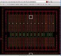
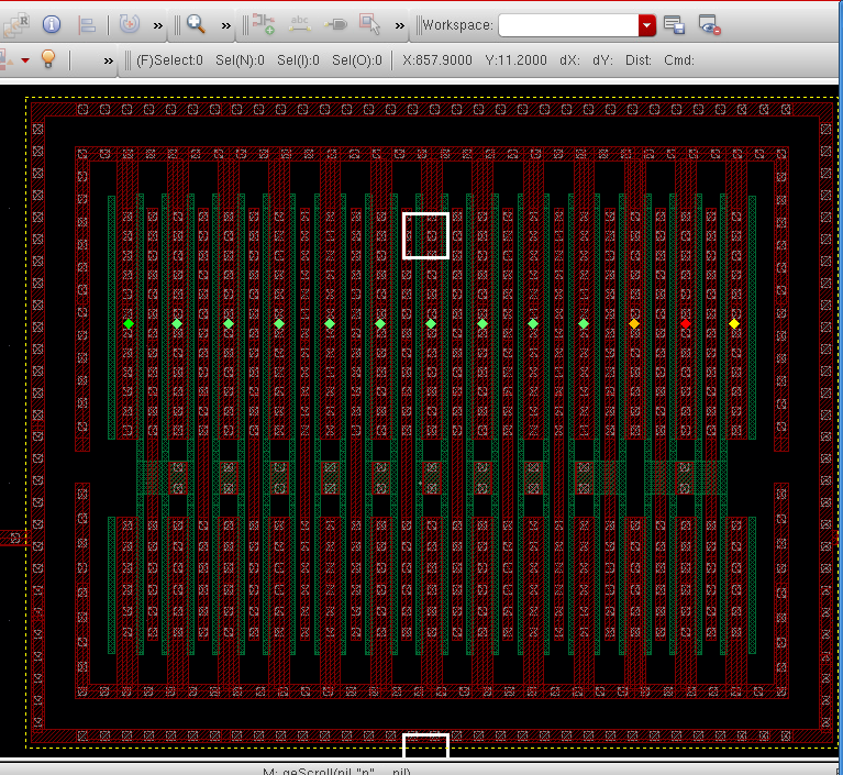
Can you help me explain why the current is only concentrated on one finger only, thus exceeding the allowable current in that given size of metal?
I thought that current throughout the fingers of the MOS is the same

By the way, the image is a sample of a buffer.

Note: Red mark denotes the area wherein the area that sinks largest current in the entire cell
 

The structure doesn't really speak to me in terms of
circuit function, but I'd guess there is one given that
the poly is broken up.

I see what looks like a source finger that feeds two
drains, each also fed by another source and so on.
So I'd call a unit drain current at the root of the
source stripe, unidirectional, defined by some load
of your estimation.

Current enters at the root and the first contact
sidewall is your probable choke-point. You would
apply a construction-analysis-based, worst cased
cross section at that point (A). Then your knowledge
of the load, and the duty factor at which you throw
that current, would give you I for purposes of Javg.

You probably ought to accommodate the reality that
finger current distribution has some nonuniformity, but
I don't often see this done. At any rate if you only have
the aggregate output current, then you'd apportion it
between fingers using your best judgment or data.


hi dick_freebird,

I understand little in this reply. Can you please elaborate this, in a much simpler terms?
You know, I am still a newbie when it comes to CMOS concepts.

I will appreciate it a lot.

Thanks.
 

Are all fingers supposed to be conducting current uniformly?

The layout shown seems to be incomplete - I assume that RED is metal1 - then where is metal2, via1, etc?
For example, if only that finger (with high current) is connected by via1 to metal2 - that would explain your problem (assuming that parasitic R extraction is done properly).

Very often, at the device level, R extracted network is not correct (for example, where and how device instances/fingers are connected to metal1 R network), and thus one can see some strange effects.

Max
-------
 

Hi timof,


I disected the view of the buffer picture on the start of this thread.

You can consider the following images. They are arranged from base layer up to metal 3 respectively

up_to_M1.PNG

M1_to_M2.PNG

M2_to_M3.PNG


That's what I can show.

Hope these images can be of help.

Thanks!
 

This does not seem to be a simple inverter, it's a more complex circuit - can you show a schematic, and where the schematic elements are located on the layout? (also - input / output ports for the current)

Without that - how can one understand the current flow...
 

This does not seem to be a simple inverter, it's a more complex circuit - can you show a schematic, and where the schematic elements are located on the layout? (also - input / output ports for the current)

Without that - how can one understand the current flow...

@timof,

Here it is.

schem.PNG

M1_to_M2_detailed.png

:)
 

OK, now it seems to be clear.

The input inverter has four poly fingers (four MOS devices in parallel) for NMOS and four for PMOS - on the right side of the layout.
PMOS has wider gate, so it is on the top (NMOS is on the bottom).
So, you are simulating PMOS transistors, as far as I can tell.

Now, the four fingers are supplied by three M1 lines from the Vss (metal on the top side of the layout).
The middle M1 line (for input inverter) supplies the current to two device fingers, while the left and right lines - to one line (each).
That's why the current in the middle M1 finger is ~2x larger than the current in the left and right M1 finger - it is shown by red, vs yellow for left and right fingers.
It would be helpful if you would include the color bar (showing what color corresponds to what current (density) level).

In fact, I think that the left M1 finger (for the input inverter) supplies current to one finger in input inverter and to one finger in the output inverter.
The current per finger in output inverter is lower than that in the input inverter (green color - in the output inverter - corresponds to lower current than yellow color - in the input inverter), that's why the current in the first M1 finger is higher than that in the third (rightmost) finger, but smaller than the current in the middle finger. It seems to be orange-like color...

That being said - what operating condition are you analyzing?
In steady-state, the currents should be zero...

Please note that this color coding for currents, while being correct qualitatively, may not be very accurate quantitatively, because of somewhat crude model for R (resistance) extraction.
The current densities in metal lines will not be uniform due to distributed effects...

Max
------
 
  • Like
Reactions: meeyaw

    meeyaw

    Points: 2
    Helpful Answer Positive Rating
@timof


Now I understand why that the current is highest on that one finger. This is due to sharing of the M1 middle finger on the input inverter. Great explanation indeed.
So in my end, the solution to resolve that high current density issue on that M1 is to increase the width of that affected M1, right?

About the current distribution on the second inverter, it seems that they have "equal" current flowing on each of the M1 finger. I noticed also that the VIA of M2 to M3 (pink small squares) covered the second inverter area and none on the input inverter. If I have to add that VIA on the input inverter side, is it possible that the current at each M1 inverter finger will also become "uniform" ?

By the way, the conditions is frequency 400MHz at 125°C (dynamic power analysis).

Thanks a lot :-D
 

Now I understand why that the current is highest on that one finger. This is due to sharing of the M1 middle finger on the input inverter. Great explanation indeed.
So in my end, the solution to resolve that high current density issue on that M1 is to increase the width of that affected M1, right?

The short answer is - yes. This may not be that easy in practice, or may be time-consuming, for the layout engineer.
Ideally, the widths of metal lines should be selected so as to insure the uniform current density (thus - minimum resistance AND minimum current density).
AND - without increasing the parasitic capacitance of interconnects.

About the current distribution on the second inverter, it seems that they have "equal" current flowing on each of the M1 finger. I noticed also that the VIA of M2 to M3 (pink small squares) covered the second inverter area and none on the input inverter. If I have to add that VIA on the input inverter side, is it possible that the current at each M1 inverter finger will also become "uniform" ?

Current densities in the metal fingers of the second inverter are much lower (why?) - so, while similar (current imbalance) effect is taking place over there - it is much less pronounced (in absolute terms).

Adding via2 over the input inverter may help (for current crowding in metal2) - but you would need to plot current densities in all metal/via layers to do the proper optimization.
But, this would not help with current crowding in the middle M1 finger - it is set by the transistors (two transistor per finger - versus one transistor for the left and right fingers).

By the way, the conditions is frequency 400MHz at 125°C (dynamic power analysis).

I am not familiar with "dynamic power analysis" - can you explain it, briefly?
In particular - is it done based on post-layout simulations (accounting for the parasitics)?

Why there is no current / power in the drains of NMOS and PMOS, and no current/power in the source of NMOS on your plots?
Are they not conducting current?
 

Dynamic Power Analysis - it a power analysis wherein the CMOS is in switching mode, changing state from logic 1 to logic 0, like those in clock circuits. The power consumed by the CMOS in this mode is called dynamic power.

Why there is no current / power in the drains of NMOS and PMOS, and no current/power in the source of NMOS on your plots?
Are they not conducting current?

The tool has separate rail analysis with VCC and VSS rails. The image shows VCC rail analysis. For the VSS analysis, the same also happens on the vss side (lower portion of the buffer layout)
 

"Power" is not the same thing as "electromigration" - does your "power analysis" tool performs also "electromigration analysis"?

And what about nets other than power/ground - for example, the net connecting the drains of NMOS and PMOS devices? - current there is similar to current in power nets (at the cell level)...
 

I know that power is different from electromigration.

Sorry for somewhat misleading you.

The one that I have been analyzing is electromigration on the power rails caused by the currents flowing into the metal tracks when the CMOS is in switching from logic 0 to 1 (hence the reason i associated "dynamic power analysis" ). The Electromigration Analysis tool requires me to input this variable: power, temperature, process corner, frequency and activity factor. The power I used in my analysis is the power that I came up while simulating dynamic (switching) power in the test circuit.

For nets other than the power rail (a.k.a signal lines), the tool doesn't take account for that as the tool that I am using is designed for electromigration analysis on the power tracks only.

I hope I make some point clear.

Thanks.
 

Thanks for the explanation.

I have a few questions, on your electromigration analysis.

What do those diamond-shaped markers mean? Does their color correspond to the current in the devices, on in M1 lines?

Due to distributed effects (complex connections between metal layers), current density in the metals / vias is highly non-uniform - is this non-uniformity taken into account somehow in this analysis?

For example - current density in M1 would be smaller if M2 bus would cover M1 "more fully". There is a lot of open space, not covered by M2...
Another thing - connections of drains of the transistors (internal node) is really poor, as compared to power net connections (only one narrow bus in M2) - I expect the current densities to be much higher than in the power nets...

If you care about details of the metal routing inside the cell (for current density / electromigration, current uniformity, low resistance, etc.) - then simulation tool like this might be handy...

If, to the contrary, your focus is on the power net (and not on the individual cells) - then the details of the R network and current densities inside the cells can be ignored...
 

One thing missing from all of this discussion, is the duty
factor of the finger current. In an individual FET this
current will be more like an impulse, when you're driving
other CMOS loads, and you want to base your current
density compliance analysis on the time averaged (DC)
value. Only at extremely high frequencies will the average
approach 50% of peak value.

It's surprising to me that an internal buffer node would
ever come close to caring-about. You might step back a
bit and look at the assumptions input to this process,
and whether the "largest current" is trivial, significant-
but-tolerable, or actionable.
 

Dick -

Thanks for your input.

time dimension that you are talking about is perpendicular to the spacial dimensions.
The original question was on current non-uniformity across fingers in MOS transistors (inverters, buffers).
I don't think that this non-uniformity is related anyhow to the transient effects.
A metal finger feeding two transistors will always have ~2x current than a finger of the same width and topology that is feeding one transistor, be that DC or time-dependent current - would you agree?

The plot of the current (densities) - colored markers - did not even show the color range or the scale of the currents.

I assumed, implicitly (probably too naively), that people do the proper analysis for electromigration - i.e., comparing DC simulation results against DC current density rules, transient simulation results (post-processed in a proper way) - with average or peak or RMS current density rules, etc.

I do not agree that current density should only be checked for time average current values - peak current, RMS current are important quantities as well.
As an example, if a current in a net is bi-directional, its average value is close to zero, but RMS or peak current may be too high.

Regarding internal or external buffer nodes - I am not a specialist in electromigration, but it seems to me, based on symmetry considerations ("symmetry considerations" is a very powerful thing in physics), that if one analyzes individual fingers of a transistor connected to the power net - since the charge is not stores in teh device, and equal current has to pass through the internal node/net, this internal net has to be analyzed as well - do you agree?

Also, as far as I know, people do care about electromigration in internal nodes (standard cells, signal nets, etc.), here is an example of such a paper.

Regards,

Max
-----
 

Thanks for the explanation.

What do those diamond-shaped markers mean? Does their color correspond to the current in the devices, on in M1 lines?

Due to distributed effects (complex connections between metal layers), current density in the metals / vias is highly non-uniform - is this non-uniformity taken into account somehow in this analysis?

The diamond markers is only an indicator of regions (MOS finger) of high current density. The tool doesn't account for non-uniformity of the current flow in that finger.
The color scheme of the tool is based from the current density criteria I have set based from the tool manual for usage.

Thanks for the inputs.
 

Status
Not open for further replies.

Part and Inventory Search

Welcome to EDABoard.com

Sponsor

Back
Top