Okada
Banned
I need help in designing Eagle footprint for Capacitor.
I want to design eagle library for
Samwha Electrolytic Capacitors of the following values
1000 uF 63V
1000 uF 35V
1000 uF 25V
1000 uF 16V
Please mention what is
PhiD
Phid
alpha
beta
Where is L, mentioned
Provide an example to read the pages 89 and 90 of the attached datasheet and get the calculations for making footprint for 1000 uF 63v Capacitor.
How to draw a Circle in SilkScreen layer in eagle ?
Edit: I found the Circle tool. Now please explain with an example how to get the dia and pin distance for 1000 uF 63V from the datasheet.
Edit 2: I found PhiD and L in the table. What is Phid ?
Edit 3:
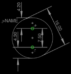
Got the values
For 1000 uF 63V
PhiD is 16
P is 7.5
Phid is 0.8
alpha = 0.5
beta = 2.0
Pin distance is 7.5 +/- 0.5
I want to design eagle library for
Samwha Electrolytic Capacitors of the following values
1000 uF 63V
1000 uF 35V
1000 uF 25V
1000 uF 16V
Please mention what is
PhiD
Phid
alpha
beta
Where is L, mentioned
Provide an example to read the pages 89 and 90 of the attached datasheet and get the calculations for making footprint for 1000 uF 63v Capacitor.
How to draw a Circle in SilkScreen layer in eagle ?
Edit: I found the Circle tool. Now please explain with an example how to get the dia and pin distance for 1000 uF 63V from the datasheet.
Edit 2: I found PhiD and L in the table. What is Phid ?
Edit 3:
Got the values
For 1000 uF 63V
PhiD is 16
P is 7.5
Phid is 0.8
alpha = 0.5
beta = 2.0
Pin distance is 7.5 +/- 0.5
Attachments
Last edited: