linuscomex
Junior Member level 3
hi.
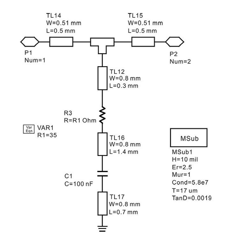
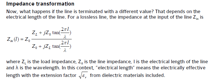
one of the most important thing to design low noise amplifier is stability.there are a lot of methods for stabilized amplifier, for example, add the resistor to drain of HEMT transistor but I can't understand why use microstrip line to connect the resistor to an amplifier? and how design microstrip length?
for clearly see an image.