Continue to Site

Welcome to EDAboard.com

Welcome to our site! EDAboard.com is an international Electronics Discussion Forum focused on EDA software, circuits, schematics, books, theory, papers, asic, pld, 8051, DSP, Network, RF, Analog Design, PCB, Service Manuals... and a whole lot more! To participate you need to register. Registration is free. Click here to register now.

Design Opinions & Critiques On My "precision" current measurement project

Status
Not open for further replies.

super7800

Newbie
Joined
Mar 13, 2021
Messages
5
Helped
0
Reputation
0
Reaction score
0
Trophy points
1
Activity points
129
hello! this is my first post here, hopefully I'm including enough information, but not too much that nobody will bother reading it.

I was wondering if anyone could take a look at my circuit for my second version of my "precision" current sensor, specifically the analog section. (TL/DR Last Paragraph). my first version, discussed Here, was a overall failure, although I did learn quite Abit from that (mainly that much of my approach was flawed), so it wasn't a total loss, and my professor seemed to agree since I did end up getting an good grade on it.

I have obviously not given up, and have since designed a second version. It is for my final project for an advanced digital systems class, so features more of a digital system than my previous attempt. it is not part of the assignment to design my own board or circuit, but where's the fun in that : ) I will admit that i'm not the best at some of the analog design stuff.

the "goal" of the project is accurate measurement of currents ranging from 1uA to 1A, with a burden of 10uV/mA and 10uV/uA, using a 10R and a 0.01R shunt. the "application" is to measure sleep currents of microcontrollers, but obviously this can be accomplished more simply, I would want my device to offer features for other "precision" current measurements. (the theoretical value for 10uV/mA is likely to have a slightly higher burden, maybe 15uV/mA)

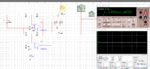
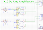
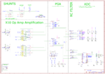
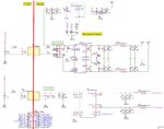
it works by using two shunts, which are amplified by a differential op amp, and then again by a PGA, and then fed into a dual channel (multiplexed) 24 bit ADC. both shunts can be measured at a relatively fast time between the two, since it has a ~8k sampling rate (ltc2442) at its lower resolution, as each shunt has their own amplification path, and the 10R can be shorted with a relay. No I don't expect to get 24 bits of usable data on this prototype, but the more usable bits the better.

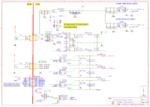
analog side is isolated from digital using a pair of dc/dc isolation modules and an spi isolator. analog side is controlled by an ICE-40 fpga, and digital from a ATSAM arm mcu. the fpga does all the signal processing tasks, the mcu handles the 240x320 color tft lcd, pc communication, and other tasks. the device is battery powered from 1s lipo, although it is not designed for maximum battery life, as its intended to be plugged into USB for most applications. also of note the pictured 10R shunt is likely to change to a lower wattage more temperature stable one.

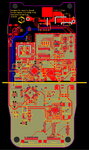
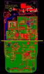
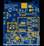
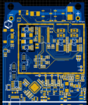
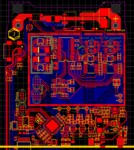
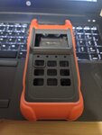
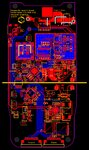
that's the brief summary, If anyone wants more information I would be more than happy to elaborate. Attached are images of the case, analog amplification, analog power supplies, PCB layout, and full PDF schematic. PCB layout has inner power/GND layers hidden. I don't expect anyone to fully or even partially review my design, but if anyone has any input on my analog section/ layout, my full design, or has a suggestion for an entirely new way to approach the shunt measurement problem, I would appreciate it, as I'd like this ~300$ prototype to at least somewhat work (lol), as I probably couldn't do a new version for awhile if this one fails catastrophically . Thanks.

EDIT: What's the problem: Specifically I want design input/ critiques on my analog frontend circuit (the circuit that does the amplification from the two shunts) and perhaps on the analog power supplies. Picture "analog section" in particular. Any critiques on my layout or any other parts of my design are appreciated. thanks.
 

Attachments

  • Analog Power.jpg
    Analog Power.jpg
    713 KB · Views: 88
  • Analog Section.jpg
    1.5 MB · Views: 59
  • case.jpg
    case.jpg
    1.9 MB · Views: 80
  • PCB V.1.5.jpg
    PCB V.1.5.jpg
    5.1 MB · Views: 72
  • Schematic_3.1 low burden current sensor_2021-03-12_01-16-56.pdf
    664.6 KB · Views: 59
Last edited:

Hi,

You missed to write what's the problem.

Klaus
 

    super7800

    Points: 2
    Helpful Answer Positive Rating
Hi,

A lot of text but still a lot of information missing.
What's the goal of the measurement device? Is it mainly to use a scope..with the big graphic display?
Is it tracing signals?
What's the idea behind it? What persons, what applications is it designed for?
How are the data processed? What algorithms?
What's the target accuracy, what precision, what resolution? ("The best" is no valid answer, because it leads to infinite effort. We need values. A good design starts with a requirement, a specification, ranges, values with units)
I miss a solid GND plane. Especially for high precision this is urgent. Your "pieces of GND" with embedded other signals is far from being a solid GND plane. (Don't get me wrong with this. Your GND in the several sections is not bad, but it does not match the effort in part selection and hardware)
The analog path is without filtering, it looks like a high bandwidth design. But the ADC has just a low datarate. I recommend to use a filter at the very input, to avoid PGA input stage overdrive by dv/dt and ringing. Do calculations choosing a suitable analog cutoff frequency. I know the ADC does internal digital filtering, but no digital filter avoid alias frequencies, it has to be filtered on the analog side.

I see many parts of your design are very good, very sophisticated... in my eyes it's the "combination" that does not match.
Did you do error calculations? Since most errors are added with the use of square...only the big errors (maybe one) count and the minor ones (even if many) only result in marginal variations.

But you did a good job. I see you read datasheets and application notes, followed the design recommendations. I see you spent a lot of time.

Klaus
 

    super7800

    Points: 2
    Helpful Answer Positive Rating
thanks for your input!

to start off, i know it might not have been clear but i did mention about the power/ gnd that " PCB layout has inner power/GND layers hidden ". i tend to hide those in pictures as i consider signal traces to be of a higher importance. on layer three in the analog section is a combination of gnd + power, with layer two being only gnd, so in many parts of the analog "cans" is effectively 3 layers of gnd (hence the via stitching in that area). attached are two images showing this (one for each inner layer, gray layer 2, green layer 3), and a rendered image as well which shows the "guard" traces and cutouts better. I should mention again that the 10R resistor pictured is likely to change to a smaller wattage one.

as to data processing in the fpga, no idea about any specific algorithms. I haven't specifically taken any courses on that, and haven't given it much thought other than "calibration data stored in eeprom, reads temperature, calculates accordingly, sends data to mcu, handles outranging, mcu tells it what "mode" its in, mode being defined as use both shunts, use one, hold pga to specific gain, handle everything automatically and store as many values as you can until MCU ask for them, ETC ETC". I might have "predictive" modes where the mcu knows the approximate timings of current cycles and pre-emptively shorts the 10R shunt, but im basically going to decide and design all that after I have the hardware operational.

"application" is both for general "precision" low current low burden measurements (1uA to 1A), and more specifically sleep/ wake currents of an mcu system.

capabilities are accurate readings of values of 1uA to 1A, with a goal of 5 usable (significant) digits.

to answer the display question and interface question, i wasn't originally going to go with a color display, just a black and white to display numbers and a menu, but the more that i looked at what was available and thought about what i wanted the device interface todo, (also case has a nonstandard size screen), I settled on a 240x320 color tft lcd (~2.2") that was the only one I found that would kind of fit and had documentation that was actually usable and documented. so when I finally selected that screen, I decided that it will plot values, display current values, and it has 256MB of flash to store values for datalogging/ plotting etc, and would be able to determine rough timing analysis jobs, i.e. how long was current above/ below a certain threshold. Although due to my rough calculation on power consumption, the battery life on the 1S lipo wont be great, which since I class this as a "bench" device in a "mobile" case wont be an issue. basically the idea is that it doesn't require a pc and software to do its job well, so easy to setup for quick measurements, but would have more powerful pc based software.

I will look into a filter, and post an updated "frontend" sometime tomorrow. thanks.

as for error issues, the x10 amplification uses a quad resistor package, the lt5400, which matches 0.01% with a 7.5% tolerance on values. The shunt 0.01R is 0.1%, and the 10R is about 1%. the shunt tolerance shouldn't be an issue, taken care of by software calibration, but perhaps the 10k, 100k pairs in the lt5400 at 7.5% tolerance might be an issue, even though they very closely match. i'll have to calculate out though if the 7.5% can be software calibrated out or not. rough calculations tell me gain vary from x8 to x12. as for the op amp in the x10 stage, I needed a "fully differential" op amp, and after a day of looking decided I might use a ADA4945-1, with a ±115 μV maximum offset voltage from −40°C to +125°C, which might be an issue for measuring 1uA, a 10uV signal, but since I'm reading the temperature, might be partially calibrated out.

I believe that should clarify? hopefully I didn't forget anything important again. thanks.
 

Attachments

  • PCB_V1.5_2021-03-13_03-26-46-1.jpg
    PCB_V1.5_2021-03-13_03-26-46-1.jpg
    193.4 KB · Views: 68
  • PCB_V1.5_2021-03-13_03-27-11-1.jpg
    PCB_V1.5_2021-03-13_03-27-11-1.jpg
    194.8 KB · Views: 79
  • pcb v.1.5 render.PNG
    pcb v.1.5 render.PNG
    216.9 KB · Views: 75
Last edited:

ADA4945-1 seems unsuitable for the application. It makes no sense to use a 100 MHz differential amplifier for low kHz analog measurements. The bipolar amplifier has relative large bias and offset currents and might be even unstable with 10 kohm level feedback network.
 

    super7800

    Points: 2
    Helpful Answer Positive Rating
ADA4945-1 seems unsuitable for the application. It makes no sense to use a 100 MHz differential amplifier for low kHz analog measurements. The bipolar amplifier has relative large bias and offset currents and might be even unstable with 10 kohm level feedback network.

what would you propose I do differently? I selected the amp in question due to its seemingly superior ±0.1 μV/˚C Offset Drift and its Input voltage noise of 1.8 nV/√Hz. the LTC6363 was another candidate I had selected. is there a specific reason you think it would be unstable with a " 10 kohm level feedback network "? I could do a more detailed analysis on the problem if you think that it could be one. I am definitely open to suggestions if you or anyone else has an idea for a better amplification frontend. thanks.
 
Last edited:

Total input referred noise density in your circuit is several 10 nV/√Hz generated by 10k resistors, resistor noise itself plus amplifier noise current related. To utilize the amplifier noise performance, the feedback network must have much lower resistance level. Stability problems are brought up by amplifier input pole, but can be easily overcome by placing a small capacitor in parallel to Rf.

I would opt for a general purpose instrumentation amp rather than a multi 100 MHz high speed amp.
 

    super7800

    Points: 2
    Helpful Answer Positive Rating
your right, I feel like I should have thought of that before. I figure I could use a LTC2055HV in the pictured configuration, would anyone have any critiques on that? Also, do you think that it would be "worth it" (i.e. tangible benefit) to do any filtering on the voltage reference, perhaps similar to this design note? I am already using a fairly high quality Alum Poly output capacitor. Design Note. thanks.

EDIT: just realized that since the two resistor networks match their resistors closely, but the package to package is about ~7.5%, I would probably have to change the package to all same value.
 

Attachments

  • multisim differential.PNG
    multisim differential.PNG
    152.9 KB · Views: 112
  • x10 2055.PNG
    x10 2055.PNG
    110 KB · Views: 75
Last edited:

thanks to everyone who has responded so far, your input has helped me greatly on my project.

I believe that I have now reached my final design, with likely very little left to change (I might replace the x10 stage with something else, or look into more filtering). I have added two more fairly low cost ADC's (16 bit), that I'm using just for their high sample rate, and (almost) couldn't care less about their actual accuracy as long as their values can show a trend. I'm using them in the FPGA to help implement some data algorithms, and outputting a "compressed" sample rate to the ARM micro for graphing, analysis, and storage. The ltc2442 is still the main ADC.

As before, I'm curious on anyone's opinion on reference filtering, do you think that I should do any filtering on the voltage reference, perhaps similar to this Design Note? thanks.

also as before if anyone has input on my analog section it would be appreciated, thanks. specifically on the x10 stage. i've thought about changing it to an instrumentation amplifier (single package) as was suggested, instead of the solution I'm currently showing being used in my schematic, but I am unsure.

The only other change is to the analog power section, where I'm using adjustable regulators now, and a power sequencer. I have also added a second reference for the Vcm. I may also add some form of filtering to the reference aforementioned.

I do not expect to reach the goals of my project on this revision, and would expect to have to design at least one more version before I reach my goal. I will likely not fully populate this prototype's analog section, probably removing the 10R shunt and its accompanying components from the digikey order, but if the prototype exceeds expectations I would order the additional analog parts. I will likely order the PCB's and parts for this prototype sometime this week, perhaps on 3/25/21. any input on my design is appreciated, thanks.

attached are new design files. the PCB has the two inner layers hidden, GND and power + GND.
 

Attachments

  • Analog Power.png
    Analog Power.png
    237.4 KB · Views: 66
  • Analog System.png
    Analog System.png
    398.2 KB · Views: 68
  • pcb analog render.PNG
    pcb analog render.PNG
    205.7 KB · Views: 70
  • pcb analog.PNG
    pcb analog.PNG
    292.8 KB · Views: 69
  • Schematic_3.2 low burden current sensor.pdf
    745.7 KB · Views: 86

Status
Not open for further replies.

Part and Inventory Search

Welcome to EDABoard.com

Sponsor

Back
Top