Continue to Site

Welcome to EDAboard.com

Welcome to our site! EDAboard.com is an international Electronics Discussion Forum focused on EDA software, circuits, schematics, books, theory, papers, asic, pld, 8051, DSP, Network, RF, Analog Design, PCB, Service Manuals... and a whole lot more! To participate you need to register. Registration is free. Click here to register now.

Common base rf amplifier problem

Status
Not open for further replies.

RadioHobbies

Newbie level 4
Joined
Sep 22, 2022
Messages
7
Helped
0
Reputation
0
Reaction score
0
Trophy points
1
Activity points
62
common base.jpg

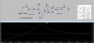
Trying to adjust the bias of the above circuit , I noticed that the 37 k pot need to be at its highest value ,
ie : the circuit need more positive voltage on the base
then the maximum gain I've got was when I connect the base to the ground (positive terminal by removing resistors & cap)
That gain wasn't enough though
I thought of the collector should have a resistor to make the pot have a center point
I added a 2.7 k resistor to the circuit in the series with the collector (and a 103 cap for passing the signal to the ground), that was right ,
the pot now have a center point where the gain reach its maximum value ,
then get decreased when the pot value exceed some point but in that arrangement , the gain became
very low (less than before)

I am not familiar with common base amplifiers

any suggestions please ?
 

To understand 2.7k resistor effect, observe Vce versus base bias. You'll see that gain collapses when the transistor saturates, just expectable. Adding voltage drop to the collector circuit creates no advantage, just a bad idea.

The main bias effect seen in the original circuit is that transconductance increases with transistor current. As long as source impedance is lower than 1/gm, increasing gm will increase circuit gain. Apparently this is the case in your circuit. As we don't know the impedances and winding ratios, we can't forsee if increasing Ic further would still increase gain.

Setting Vbc = 0 keeps Vce above saturation limit, but reduces undistorted output voltage swing. Even if you observe highest gain with this bias setting, receiver blocking behaviour becomes worse.

That gain wasn't enough though
Consider that gain of a single BJT stage is limited.
 
The principle of common-base mode is that the incoming signal changes voltage at the emitter (instead of the base terminal). In effect this changes the B-to-E relationship just the same as if the signal were applied to the base terminal.

Common base mode permits low input impedance. Your coil is suitable for providing a signal.

It's okay to apply 0V ground to the base. A bias resistor is unnecessary (although there's nothing wrong with installing a safety resistor). The key is to carefully adjust voltage of the negative supply rail. It may take time to find that narrow window where full gain is available.

common base NPN 100 gain (base to 0v gnd) 5mV sine amplified to 1V .png
 
Thanks guys for the suggestions
I have to mention that I design that circuit to work on Medium Wave band range 530 - 1600 KHz
also I've forgot to describe my RF transformer at the output

its a Toko coil , I've rewound it as the following :

primary coil (transistor side) : impedance is about 23 uH (38 turns) ,, <--I think the problem is here ?
Secondary coil : the whole impedance is about 300 uH (137 turns)
* why 300 uH ? to be equal to the loopstick's impedance (so that all tuned circuits are equal) .
 

To get gain out of a common base amplifier the impedance seen by the collector must be higher than the emitter. Simplistically the emitter current and collector current are equal so the higher the collector impedance the higher the gain. From your circuit it looks like you have the low impedance winding of the output transformer connected to the collector.
 
I have modified the output RF transformer by increasing the impedance on the primary coil (transistor's side) to 160 uH (I wonder if that enough in case Medium Wave)
the gain have increased noticeably , the base is still need to be connected to the battery's positive terminal (no center point for the pot ).
 
Last edited:

I think you are confusing impedance with inductance.
The inductance and tuning capacitance decide the resonant frequency (1/(2*Pi*sqrt(L*C)). The impedance matching depends on your needs, more coupling (more turns on the un-tuned side) will increase the amount of signal passed through but at the same time will reduce the 'Q' factor which is a measure of how sharp the tuning will be. As the tuning becomes less sharp, the less of the signal you want will be selected so you have conflicting effects.

I'm going to make a wild guess at optimal inductors for you:
The larger of the two coils should be identical and 160uH is a reasonable value.
The emitter input coupling coil should be about 5 turns.
The collector output coil should be about 10 turns.
The output tap from the ground side of the larger output coil should be at about 5 turns.

This assumes the two tuning capacitors are somewhere in the region of 300pF each. If you are using a dual-gang tuning capacitor you will also have to make at least one of the coils adjustable so you can match their resonant frequencies.

Do not place the input and output coils close together and certainly not in line with each other as this could cause oscillation.

Brian.
 
Try using the attached schematic. I kept the values of the resonator inductors that you have, but I did reverse their primary and secondary windings, to get low input and output impedances of the amplifier.
The gain is greater than 20dB for the entire frequency range, but most probably for the built amplifier this will be smaller .
 

Attachments

  • CB_BJT.jpg
    CB_BJT.jpg
    646 KB · Views: 113
OK guys all of that are fine , I am just confused about one thing
how to make the variable resistor at the base to get a center point
as I mentioned in the first post , I achieved to do that only when connected a resistor in series with the collector
and that was a bad idea as mentioned bellow
To understand 2.7k resistor effect, observe Vce versus base bias. You'll see that gain collapses when the transistor saturates, just expectable. Adding voltage drop to the collector circuit creates no advantage, just a bad idea.
and that was right .
 
Last edited:

Status
Not open for further replies.

Part and Inventory Search

Welcome to EDABoard.com

Sponsor

Back
Top