Continue to Site

Welcome to EDAboard.com

Welcome to our site! EDAboard.com is an international Electronics Discussion Forum focused on EDA software, circuits, schematics, books, theory, papers, asic, pld, 8051, DSP, Network, RF, Analog Design, PCB, Service Manuals... and a whole lot more! To participate you need to register. Registration is free. Click here to register now.

BJT with really tight tolerance on hfe?

Status
Not open for further replies.
Onsemi datasheet, but unfortunately, I read it wrong. hFE 300 is maximum. Thanks for clarifying.
 
  • Like
Reactions: treez

    T

    Points: 2
    Helpful Answer Positive Rating
whatever the gain is, do you agree that the small signal transfer function of the error amplifier that includes the BJT will be just the same as the transfer function without the BJT, but multiplied by the gain of the BJT?
 

In my experience (decades old, at crusty 4" wafer fabs) hFE
is not well controlled - not even peak hFE. And the rolloff at
high and low currents, even less so, involving at the low end
defects and other attributes not specific to the base width.

And high hFE means narrow base width means control issues,
two implants & subsequent drive / activation in a foot-race
as it were, each having variation. Early voltage varies the
"effective" hFE with collector voltage.

Cherry-picking from an oversized lot population is a real thing.
 

whatever the gain is, do you agree that the small signal transfer function of the error amplifier that includes the BJT will be just the same as the transfer function without the BJT, but multiplied by the gain of the BJT?
I believe that is true.
So to take the BJT current gain out of the equation, convert the current from the opto transistor directly to a voltage using an amp with a gain determined largely by feedback (op amp or transistor common-emitter stage with emitter degeneration).
That way you will only have the variation in opto gain to consider when looking at loop stability.
 

So to take the BJT current gain out of the equation, convert the current from the opto transistor directly to a voltage using an amp with a gain determined largely by feedback
-the problem I the topswitch-jx expects a feedback current, not a voltage. We have to amplify the opto current and feed that amplified current into the control pin of the topswitch-jx.
 

You might use a degenerated current mirror to make a
better controlled current transfer ratio, but you have
to operate well below the hFE (@OP) as a ratio. The
opto CTR, there's big question as regards make tolerance
and aging.
 

Proper design of a darlington (degeneration resistors) and/or the use of a pnp-npn darlington will sufficiently overcome gain spread issues.
 
  • Like
Reactions: treez

    T

    Points: 2
    Helpful Answer Positive Rating
-the problem I the topswitch-jx expects a feedback current, not a voltage. We have to amplify the opto current and feed that amplified current into the control pin of the topswitch-jx.
How about amplifying the optocoupler output using a Howland current output circuit.
The current gain of a Howland circuit is a function of the resistor values.
 

thanks, though its actually a current amplifier that we need, we need to amplify a current of 100uA to 1 milliamp by seven times.
 

The best commercial gain spread opto's are typically 80<CTR<160 so this puts a variance on the gain for starters, driving an opto with a current source does nothing to compensate this effect.

Only by using a linear opto arrangement (IL300 etc) will you get a sufficiently narrow gain spread (0.9 - 1.15)
 

thanks, we can grudgingly accept the 80-160 spread of opto's, its just the 30-300 spread of hfe in most bjt's that crock's us. (due to voltage mode feedback loop tending to be less friendly to gain variance than current loop)
 

thanks, though its actually a current amplifier that we need, we need to amplify a current of 100uA to 1 milliamp by seven times.
Okay.
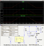
Here's an opamp circuit that multiplies the opto output current by a factor of 7 into R_Cload (the controller C input).
As can be seen, the output current is independent of the load resistance (shown for R_Cload values of 0.1Ω, 10Ω, and 100Ω).
The current gain is basically determined by the ratio of R3/R2 (set here as 7) and is largely insensitive to other circuit parameter variations including the transistor current gain.

The op amp needs to be a rail-rail input and output type.

The supply voltage can be any value within the range of the opto and op amp ratings.

Opto Current Amp.PNG
 
  • Like
Reactions: FvM

    FvM

    Points: 2
    Helpful Answer Positive Rating
Perfect solution. But as mentioned before:
"Any current amplifier with tightly tolerated gain I can think of would use considerably more components." (than a single BJT)
 

Sigh, by fitting degenerations R's to the npn opto and the other part of the darlington, the max gain can be limited....
 
  • Like
Reactions: treez

    T

    Points: 2
    Helpful Answer Positive Rating
Sigh, by fitting degenerations R's to the npn opto and the other part of the darlington, the max gain can be limited....
Thanks, but we don't know to what value it gets limited to.


Crutschow....I am mega impressed with your circuit, I sat there with pen and paper and tried to do similar, but you have well beaten me to it....your circuit is exactly what we want...its so good that I am wondering if it can be for real.
The only problem I can see is the sensed voltages being close to the rail, but that can be solved by just putting in an extra resistor, or indeed supplying the opamp from a bit higher voltage.

By the way Crutschow, I think if you tell Power integrations about your circuit they will be mega impressed with you......you have solved the issue of ridiculously wide gain variance of topswitch feedback loops with added BJT where the flyback has a vout > 20V.....this also means your circuit helps the entire topswitch family to meet standby regs for Europe when vout >20v.....The high secondary opto current can be a problem for the 0.5W regs. yOU HAVE MADE TOPSWITCH THE BEST MONOLITHIC SWITCHER IN THE WORLD.!

The only other solution is to literaly put a 8Vout mini smps on the secondary, but that's more expensive than what you show.
 
Last edited by a moderator:

Actually sorry, Crutschow’s circuit (post #32) is great but it would need a different small signal feedback loop transfer function to be derived for it. Equation 25, page 14 of the linked AN-57 document shows the transfer function for the normal topswitch feedback loop. Crutschow’s circuit is dynamically different from the controller schematic of fig23, page 14, and so would need a different equation in place of equation 25…

AN-57
https://ac-dc.power.com/sites/default/files/product-docs/an57.pdf

Crutschow’s circuit is good but has an extra gain factor brought about by R(LED)/R(pullup), and also the pole due to the optocoupler Base-collector capacitance and the pullup resistor needs to be considered. Also there is the effect of the PNP’s emitter resistor.

So Crutschow’s method is good, but the feedback loop transfer function involving it needs to be derived first.
 

Actually sorry, Crutschow’s circuit (post #32) is great but it would need a different small signal feedback loop transfer function to be derived for it.
Why? The original circuit is a plain current amplifier (with loosely defined gain), the new circuit is a precise current amplifier.
 

yes , but I am referring to the topswitch schematic of fig23, page 14 of AN-57 (linked in post #36).
This has different dynamics than what it would be with Crutschow's circuit in there. The small signal transfer function would be different. That is, different than equation 25, page 14 of AN-57.
The new transfer function would have to be derived first.
 

Sigh, by fitting degenerations R's to the npn opto and the other part of the darlington, the max gain can be limited....
Double sigh.
You can degenerate the voltage gain of a transistor but not the current gain.

- - - Updated - - -

yes , but I am referring to the topswitch schematic of fig23, page 14 of AN-57 (linked in post #36).
This has different dynamics than what it would be with Crutschow's circuit in there. The small signal transfer function would be different. That is, different than equation 25, page 14 of AN-57.
The new transfer function would have to be derived first.
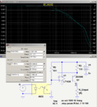
My simulations show the circuit reaches 90° of phase shift at 160kHz where the gain has dropped by over 13dB (below).
So that can be included in the loop transfer function, but I think the corner frequency is high enough that it won't have a significant effect on the loop response, other than adding a current gain of 7 to the opto gain.

Gain ckt Bode.PNG

- - - Updated - - -

.................
.......your circuit is exactly what we want...its so good that I am wondering if it can be for real.
The only problem I can see is the sensed voltages being close to the rail, but that can be solved by just putting in an extra resistor, or indeed supplying the opamp from a bit higher voltage.
..................
Yes, it's amazing how the high-open loop gain of an op amp used in a feedback circuit can greatly minimize the effects of circuit component variations as well as diode and base-emitter offset voltages, and thus improve the stability and accuracy of a circuit.

There's no problem with sensing at the rail as long as you use a rail-rail type op amp, as the one used in my simulation.
Adding an extra resistor or increasing the supply voltage won't necessarily help since R2 and R3 must be referenced to the supply voltage.
 

Thanks Crutschow, I see your point, though I am not sure if ltspice correctly simulates the base-collector capacitance of optocouplers, and I fear it will miss the pole due to that and the pullup resistor (the 931 ohm).
It might be just a case of putting a 100n from opto-collector to ground, and calculating the pole due to that and the pullup resistor (the 100n would 'drown' out the BC capacitance).
I believe you are correct and that otherwise it will just be the gain of 7, because the 133 ohm resistor doesn't come in to it, because that bit is just a current source.

I will have to think if their is a gain now to include due to R(LED) and the 931 ohm pullup. I believe there is but I will have to check.

"R(LED)", as you know, is the resistor in series with the opto diode.

Crutshchow I think your circuit is brilliant, but my brain needs to catch up now and do the small signal txfer function including your circuit and then its all great.
 
Last edited by a moderator:

Status
Not open for further replies.

Part and Inventory Search

Welcome to EDABoard.com

Sponsor

Back
Top