Continue to Site

Welcome to EDAboard.com

Welcome to our site! EDAboard.com is an international Electronics Discussion Forum focused on EDA software, circuits, schematics, books, theory, papers, asic, pld, 8051, DSP, Network, RF, Analog Design, PCB, Service Manuals... and a whole lot more! To participate you need to register. Registration is free. Click here to register now.

ADS rectifier efficiency

jdstavares

Junior Member level 2
Joined
Nov 3, 2022
Messages
22
Helped
1
Reputation
2
Reaction score
0
Trophy points
1
Activity points
167
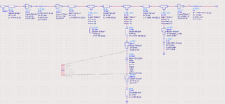
Hi everyone, I have a question regarding my rectifier circuit. I performed it in ADS software, and there I obtained an efficiency of ~30%. However, when producing the rectifier, I measured it and instead of the ~30% I obtained ~0.5% efficiency.

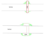
The rectifier is on a textile substrate and the conductive lines are made through conductive ink. The smd components are soldered into small copper sheets (just to ensure contact between the smd pads and the circuit), which I did not consider in the simulations, and then integrated with the ink. Nevertheless, I did not expect such a discrepancy.

Can someone give some input on what might be happening?
 
If it's a RF rectifier-looks like it- lossy elements are not used such as conductive ink, flexible PCB etc.
You had to simulate your circuit with lossy substrate and conductive ink. You might see how they impact the efficiency.
 
If it's a RF rectifier-looks like it- lossy elements are not used such as conductive ink, flexible PCB etc.
You had to simulate your circuit with lossy substrate and conductive ink. You might see how they impact the efficiency.
Thank you for the answer, it is indeed a RF rectifier. I considered the properties of the textile substrate, however, not sure if the ADS considers the substrate like a rigid PCB. Moreover, about the conductive ink, I only considered the conductivity and thickness, but are you saying that I should put more properties about it?
 
Thank you for the answer, it is indeed a RF rectifier. I considered the properties of the textile substrate, however, not sure if the ADS considers the substrate like a rigid PCB. Moreover, about the conductive ink, I only considered the conductivity and thickness, but are you saying that I should put more properties about it?
ADS Momentum can simulate any substrate since its parameters are known. This is valid for conductors and semiconductors, no matter which material you used.
But I said before, lossy substrates, carbon composite printed lines, conductive inks etc. All those materials are NOT appropriate for RF designs.
RF currents/voltages request pure conductive lines, low lossy substrates, clean and well designed cavities.
You have to get the electrical specifications of the substrate and conductive ink first then simulate to see how your design is impacted much.
 
about the conductive ink, I only considered the conductivity and thickness
So you already included the layout details, with correct conductivity of your conductive ink lines?

Can you show a screenshot of simulation model (schematic with ADS elements) and a detail photo of the measured hardware?
 
So you already included the layout details, with correct conductivity of your conductive ink lines?

Can you show a screenshot of simulation model (schematic with ADS elements) and a detail photo of the measured hardware?
Hi Volker, thank for the answer.
Yes I considered those parameters.
Bellow you can find the schematic and a pic of the measured hardware
1700583491085.jpeg


1700582816836.png
 

Attachments

  • 1700582517133.png
    1700582517133.png
    95.8 KB · Views: 59
I was going to ask about ground and vias as well, we don't see the fully metalized backside that hopefully exists.

One issue is the connection of DC output: you have connected a "random wire" to the RF routing near your diode, to measured the DC signal. But that point is carrying RF, so your DC wire will change RF properties. You should insert inductors there to block RF, and pass DC only.

missingL.png
 
I was going to ask about ground and vias as well, we don't see the fully metalized backside that hopefully exists.

One issue is the connection of DC output: you have connected a "random wire" to the RF routing near your diode, to measured the DC signal. But that point is carrying RF, so your DC wire will change RF properties. You should insert inductors there to block RF, and pass DC only.
Yes I made the gnds and vias. But regarding the wires, those wires are to perform the measurements. And in that part is already DC not RF. Besides the wires are "relaxed" in the pic, while doing the measurements they are stretched below. But do you think that they still have an impact?
 
And in that part is already DC not RF

No, you are wrong!

You connect the wire to an RF line, so it will change RF also. To extract your DC component, you must block RF by using series inductor as close as possible to the RF line.
--- Updated ---

Another comment: in your ADS schematic you have a 50nF capacitor. Such a large value will have a low self self resonance frequency, below your target frequency (2.4 GHz?), so the real component will NOT be low impedance as simulated for the ideal component in ADS.

You can try smaller value like 100pF instead.
 
Last edited:

LaTeX Commands Quick-Menu:

Part and Inventory Search

Welcome to EDABoard.com

Sponsor

Back
Top