- Joined
- Apr 1, 2011
- Messages
- 15,187
- Helped
- 2,900
- Reputation
- 5,812
- Reaction score
- 2,982
- Trophy points
- 1,393
- Location
- Minneapolis, Minnesota, USA
- Activity points
- 113,781
The error in simulation setup: It apparently uses MOSFETs without backward (substrate) diodes. They don't exist as technical devices.
In a real inverter, the diodes clamp the inductor flyback voltage to the power supply.
Yes. I neglected to install these.
After revising my simulation, the spikes are now reduced (as you state).
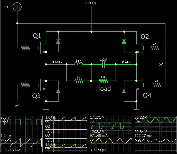
At switch-Off, the coil kicks current back up through the power supply. Hence the power supply needs to contain a component in its output stage, which can offer low impedance to this reverse current.

