Continue to Site

Welcome to EDAboard.com

Welcome to our site! EDAboard.com is an international Electronics Discussion Forum focused on EDA software, circuits, schematics, books, theory, papers, asic, pld, 8051, DSP, Network, RF, Analog Design, PCB, Service Manuals... and a whole lot more! To participate you need to register. Registration is free. Click here to register now.

Reducing noise in buck converter powering push pull inverter

Bruno5234

Newbie level 5
Joined
Feb 28, 2024
Messages
10
Helped
0
Reputation
0
Reaction score
0
Trophy points
1
Activity points
113
Hi, I designed a buck converter that powers a push pull inverter that I designed too, I want to control the voltage in the buck converter while powering the inverter, the problem I'm facing is that I can control de voltage in the buck converter pretty easy when putting a resistor load, but when I connect the inverter as a load (with a resistor load at the secondary of the inverter's transformer) I can see some high frequency noise at the output of the buck converter and I want to reduced it because I don't want to damage my microcontroller and I'm also getting a bad voltage reading because of this noise, I tried increasing the size of the bulk capacitor of the buck converter and that decreased the amplitude of the noise but made my control system slower, so I think that is not the way to solve the problem. Any ideas?
This is the schematic of my circuit:
Buck converter:
1709089894705.png

And this is the PCB I designed:
1709089952401.png

Push Pull Inverter circuit:
1709089982639.png

Push Pull Inverter PCB
1709090000246.png


I don't know a lot about PCB design so I probably made a mistake with the design
The Buck converter is control by a PWM of 32 kHz frequency, the push pull inverter is working with 200 kHz of frequency
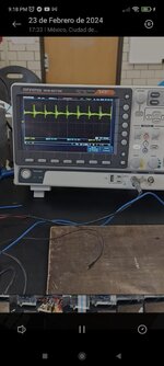
The noise I'm getting is this:
WhatsApp Image 2024-02-27 at 9.20.21 PM (1).jpeg

The frequency of the noise is the double the frequency of the inverter, so I think the problem has to be the inverter
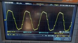
I don't know if this provide some extra information but this is the waveform I get at the secondary of the inverter
WhatsApp Image 2024-02-27 at 9.20.21 PM.jpeg

The transformer I'm using for the inverter is a toroidal transformer designed for the frequency of the inverter

Please let me know if you need extra information

Thank you for answering :)
 

Attachments

  • WhatsApp Image 2024-02-27 at 9.20.21 PM (1).jpeg
    WhatsApp Image 2024-02-27 at 9.20.21 PM (1).jpeg
    95.6 KB · Views: 33
  • WhatsApp Image 2024-02-27 at 9.20.21 PM.jpeg
    WhatsApp Image 2024-02-27 at 9.20.21 PM.jpeg
    71.4 KB · Views: 41
Hi,

schematics and PCB circuits don´t match.

If you don´t want to fool us: show matching informations. Circuits need to match, as well as designators and part values.
Everything else leads to confusion and consumes a lot of time.

Klaus
 
... also wich transformer are you using. It looks like is not on the PCB, so leakage inductance will depend on your setup, limiting tranfered energy. Also, the transformer might simply not be suitable for a push-pull topology or operating frequency. What's your target output wattage and voltage? Your scope pictures hard to read.
 
Hi,

schematics and PCB circuits don´t match.

If you don´t want to fool us: show matching informations. Circuits need to match, as well as designators and part values.
Everything else leads to confusion and consumes a lot of time.

Klaus
I'm sorry, this is the circuit of the PCB:
Buck.png

Inverter.png
 
... also wich transformer are you using. It looks like is not on the PCB, so leakage inductance will depend on your setup, limiting tranfered energy. Also, the transformer might simply not be suitable for a push-pull topology or operating frequency. What's your target output wattage and voltage? Your scope pictures hard to read.
Hi, I'm using a transformer that I made myself, it's a step up toroidal transformer with center tap, the output wattage is 100W and voltage is at maximun 1600 Vpp, the ratio is 1:40, max voltage at the input is 20 V
 
Please verify what you expect.

565 V rms, 1.77 A rms secondary or is it 100W VAR?

magnitude 565/1.77= 320 Ohms sec. with 1:80 per centre tap is 320/80² = 50 mohms primary load which needs a FET far less for RdsOn

Yet 2SK3651-01R is 0.1 Ohms max at 25'C !!

If you eliminate the Buck then you can reduce the turns ratio, and raise the RdsOn required with more FETs in parallel.
 
Last edited:
this approach for making an inverter does not work for reactive loads, ONLY resistive loads

even the X L of the Tx will upset your operation at lighter loads
 
Please verify what you expect.

565 V rms, 1.77 A rms secondary or is it 100W VAR?

magnitude 565/1.77= 320 Ohms sec. with 1:80 per centre tap is 320/80² = 50 mohms primary load which needs a FET far less for RdsOn

Yet 2SK3651-01R is 0.1 Ohms max at 25'C !!

If you eliminate the Buck then you can reduce the turns ratio, and raise the RdsOn required with more FETs in parallel.
I need the buck
 
Hi,

You want to remove the noise...
but first things first:
* is the INV output as expected? in magnitude and waveform?
* are the voltages (DC, average) as you expecting them? Or are they lower than expected?
* where exactly in the PCB layout did you connect the scope´s GND and the scope´s tip?

***
You write "PWM_INV". But it is no pulse width modulation signal.
--> It has to be a continous 50% duty cycle square wave.
Only a short time wihtout toggling may cause your transformer to saturate. Even a small deivation form 50% may cause the transformer to saturate.
I don´t know how your signals look at start up. Is the timing in a way that it prevents saturation?

I´m busy, thus it takes maybe 10h+ to be back.

Klaus
Hi,
Yes, the magnitude is correct, the waveform its acceptable, the DC voltages are correct, I connected the scope's GND at the GND connection of the Buck's output, the tip of the scope it connected to the output terminal of the buck.
And yes, the PWM_INV terminal its a square wave with 50% duty, the label is incorrect but the signal its 50% duty, the IR2104 adds a dead time in orden to properly turn on and off both MOSFET.

I also checked the signal at the drain of both MOSFET and it seems like the noise at the buck its produce only when both MOSFETs are off (the dead time) and that corresponds to some spikes I can see at the MOSFET drain, I attach the image, here I have the Buck at 5V, the yellow signal its the drain, the green its the output of the inverter
WhatsApp Image 2024-02-29 at 8.26.14 PM.jpeg

Maybe a snubber should reduce the noise? adding a capacitor in parallel with the drain to source of the MOSFET seems to reduce the spikes but also deforms the signal at the drain (I know I need to add a resistor to make a proper snubber, but I just wanted to gather some information), as far a I know I should expect the signal of the drain to be close to a square wave from 0 to double the voltage of the Buck's output
This is the waveform when adding a 10nF capacitor
WhatsApp Image 2024-02-29 at 8.26.56 PM.jpeg


Thank you for your time
 
I need the buck
You didn't answer https://www.edaboard.com/threads/re...wering-push-pull-inverter.410205/post-1769663

Measure your deadtime, DT both nominal with +/- worst case Vcc and Temperature and estimate variance from component tolerances. There may be skew each channel for some reason.

In order to reduce "DT" to a minimum , but you need to define component tolerance margin to prevent "shoothru" catastrophic failure. You can add an RC snubber at some cost in efficiency, heat etc.

Something seems to be off spec; or it just looks that way with 10% DT.
200 kHz = 5 us compared with 0.52 us +/-25% DT

Snubbers can be R, RC, RD, RLC

Consider Rsnb= 10 to 20x rated load R with a suitable Cs to match X(f)= 10% of Rsnb at fo = 5 MHz?

I suggest:
Then add series L to match Cs at fo to notch out the resonance with a Q of 10. and 10% of rated load during DT.

The RC snubber one reduces phase margin. The RLC depends on stability of fo under environmental, component, stray C and Vcc extremes. What level of distortion and EMI is acceptable?

1709327405393.png


Adding 10+ pF // Rg to Nfet ought to reduce DT. Rg & Ciss are factors


ALso Toshiba says 2SK3561 is not recommended for new designs.
 
Last edited:
Hi,

you need to properly bypass the transformer_DC supply at the inverter board. At least a low ESR 100uF in parallel with an 1uF ceramics.

***
And we need to see photos of your wiring.
You have a lot of GND connections, they may cause GND loops.

Klaus
 
Hi,

you need to properly bypass the transformer_DC supply at the inverter board. At least a low ESR 100uF in parallel with an 1uF ceramics.

***
And we need to see photos of your wiring.
You have a lot of GND connections, they may cause GND loops.

Klaus
Yes but not all low ESR caps are the same . The "best" Tau= seems to be the "Wurst" 22 mΩ max * 100 uF = Tau = 2.2 us or ~~ 500 kHz not much help for 5 MHz
He does mention 220 uF low ESR on schema. It's mostly in the magnetics and ESL.

 
Last edited:
Hi,

I agree with the 5MHz ...

but where are the 5MHz from? I can´t find any information from the OP about 5MHz.
You say "the best Tau seems to be the worst" .. so does this mean a capacitor with higher ESR is better regarding ripple suppression?

And you ingnored my "parallel 1uF ceramics" which "takes over" the filtering at a bit above 5MHz.

Klaus
1709342748104.png

Look above and see 1 us/ div and number of cycles / 1u div OK maybe it's 6 MHz !!!

I only ignored it, after I quickly analyzed it on a nomograph. 0.1uF won't help here. But I was wrong the lowest ESR e-caps have the best chance at 5 MHz.

1709335917591.png

It takes more time to show you though. ...

and more time to explain how to read SRF by the intersection of the observed fo and the LC values at any impedance ratio above Q
so this will be a quick summary.

Q is the reactive to real power ratio depending on series or parallel Qs= X/R , Qp = R/X

The impedance ratio is same as Power Ratio since both are proportional to shared I² at resonance where XC(f)=XL(f)

Yet we do not know the layout impedance at resonance unless we know exactly which 220 uF cap is installed and how the current path looks between RLC.
But I see the low nH values which suggests its not too bad but maybe can be damped if it is a parallel resonance during DT and series RLC when conducting.

All parasitics can be modeled as the pF/cm and nH/cm. 50 Ohm strip line as I recall is 6.8 nH/cm and 2.6 pF/cm roughly

So you can find exactly which cap. ESR and trace Effective Series Inductance (ESL) are resonating at 5MHz. Then you have the intersection or RLC at f and and see the Q value or visa versa.

0.1uF doesn't do much at 5 MHz as much as the 220 uF if it's SRF is > 10 MHz I am assuming will be close....
Not all low ESR caps will have the same break point but Tau is generally between 1 and 10 us in this voltage and size range.

ESL from FET RdsON, Cap ESR can be drawn on the graph if you know them

Deadtime resistance at 5MHz on scope depends on RLC which depends on Cap ESR, FET RdsOn,
ESL which depends on parasitic trace width and thickness to some extent per unit (pu) length
Parasitic capacitance depends on width and height to nearest ground and Er, so W/H ratio 6.3nH/cm for typ. signals and less for power traces.
For C is W/H to nearest ground plane. varies a lot but for 50 ohm gnd plane around 2.6 pF/cm
 
Last edited:
Look above and see 1 us/ div and number of cycles / 1u div OK maybe it's 6 MHz !!!
Makes sense.
I didn´t look this way. I guess we have different ways to look at things. And with differtn ways I just mean different ways, not right or wrong.
There is a reason why I didn´t look this way: It´s because I don´t try to cure the symptom, but to remove the cause. If possible. I first want to understand why the "noise" is generated.

0.1uF won't help here.
Where do the 0.1uF come from?

and more time to explain how to read SRF by the intersection of the observed fo and the LC values at any impedance ratio above Q
While I do understand what you want to say. And I agree with it regarding LC. But on electrolytics we talk about ESR and not ESL.
I don´t deny that ESL exists, but with electrolytics the R dominates over L. R means energy becomes dissipated as heat. L means energy becomes stored.
A soon as energy becomes dissipated, the energy is not available anymore. not available for ringing.
L causes ringing (in combination wit a )
R dampens ringing
Q is a measure how much percent of the energy is available after one cycle.
For pure LC this is 100%, on RLC is is somewhere >0% and <100%
With RC it is zero. Zero in the meaning of of available energy of oscillation/ringing.
I know that you find sources that say Q of an RC is X/R. And it is correct. Here it gives a measure how "ideal" a capacitor works.

When you look at impedance curves of capacitors then you see that with increasing frequency, the impedance decreases. At the SRF point you see minimum value (ESR) and above resonance frequency the impedance rises due to L (ESL).
But curves of electrolytics look rater different than foil or ceramics. With foil or ceramics you clearly see the rising imedance above the SRF point, but with electrolytics one misses the rising impedance ... it rather stays at flat horizontal. It just dissipates energy. The effect of a true L (that can store energy) is missing.
For sure this differes from capacitor to capacitor.

Yet we do not know the layout impedance
True. We need the photos to get a clue.

ESL which depends on parasitic trace width
Yes. Traces on a PCB. But don´t you agree that the higher impedance will be caused by the wiring between the two PCBs.
(maybe he really uses several feed long non twisted wires with banana connectors)
And thus I recommended to use a capacitor on the inverter board (there currently is no capacitor at all) to reduce this impedance effects.

Klaus
 
Even if you do all the above - your approach will only ever be suitable for resistive loads -

consider a transformer - if you put a large L as the load, the current lags the volts by 90deg, this means you can have a pos output voltage at a time the current is flowing the other way - it is a 4 quadrant device ( the transformer - power, both real and reactive can flow either way thru a transformer ), similarly for a capacitive load - where the volts lag the current ( the other 2 quadrants here )

You should critically examine your approach - if you intend to run loads that are even slightly inductive or capacitive - you need to re-think

apologies - but I have seen many newbies go down this path . . .
 
The deadtime must be measured with Vcc and Temp to determine how to improve.
The parasitic sources need to be included on schematic with estimates.

I hope this clears up what I said before.
  1. ESR comes from the insulators at the conductive boundary, Caps, and batteries both have insulator dielectrics measured in F.
  2. ESL comes from conductors based log (W/L) ratio or nH/cm assuming estimated ratios.
  3. Parasitic C is the gap W/H ratio between conductors..
Even 1uF on Vcc won't suppress this noise on secondary AC
 
Last edited:
Thank you everyone for your answers, I'll try to give you all the information requested
You didn't answer https://www.edaboard.com/threads/re...wering-push-pull-inverter.410205/post-1769663

Measure your deadtime, DT both nominal with +/- worst case Vcc and Temperature and estimate variance from component tolerances. There may be skew each channel for some reason.

In order to reduce "DT" to a minimum , but you need to define component tolerance margin to prevent "shoothru" catastrophic failure. You can add an RC snubber at some cost in efficiency, heat etc.

Something seems to be off spec; or it just looks that way with 10% DT.
200 kHz = 5 us compared with 0.52 us +/-25% DT

Snubbers can be R, RC, RD, RLC

Consider Rsnb= 10 to 20x rated load R with a suitable Cs to match X(f)= 10% of Rsnb at fo = 5 MHz?

I suggest:
Then add series L to match Cs at fo to notch out the resonance with a Q of 10. and 10% of rated load during DT.

The RC snubber one reduces phase margin. The RLC depends on stability of fo under environmental, component, stray C and Vcc extremes. What level of distortion and EMI is acceptable?

View attachment 189072

Adding 10+ pF // Rg to Nfet ought to reduce DT. Rg & Ciss are factors


ALso Toshiba says 2SK3561 is not recommended for new designs.
I apologize for not answering completely the first reply, at first I didn't understand your question, yes, the RMS voltage is expected at most 565Vrms and the current shoud be at most 200 mArms.
I calculated a snubber using the following AnalogDevices document: https://www.analog.com/en/resources/design-notes/ccfl-pushpull-snubber-circuit.html
These are the signals at both Drains without the snubber
WhatsApp Image 2024-03-01 at 4.56.45 PM.jpeg

With the snubber, R=10ohm, C=20 nF
WhatsApp Image 2024-03-01 at 4.54.28 PM.jpeg

It needs better RC values because you can still see the ripple just with lower magnitude, but the waveform looks horrible
Hi,

you need to properly bypass the transformer_DC supply at the inverter board. At least a low ESR 100uF in parallel with an 1uF ceramics.

***
And we need to see photos of your wiring.
You have a lot of GND connections, they may cause GND loops.

Klaus
Okay, I'll do that as fast as possible and give you the images
Yes but not all low ESR caps are the same . The "best" Tau= seems to be the "Wurst" 22 mΩ max * 100 uF = Tau = 2.2 us or ~~ 500 kHz not much help for 5 MHz
He does mention 220 uF low ESR on schema. It's mostly in the magnetics and ESL.

The actual capacitor I used is this: https://agelectronica.lat/pdfs/textos/B/B41858C9227M.PDF
Hi,

I agree with the 5MHz ...

but where are the 5MHz from? I can´t find any information from the OP about 5MHz.
You say "the best Tau seems to be the worst" .. so does this mean a capacitor with higher ESR is better regarding ripple suppression?

And you ingnored my "parallel 1uF ceramics" which "takes over" the filtering at a bit above 5MHz.

Klaus
I measured the frequency and it's approximately 6.6 MHz

This is a photo of the PCB, I know I should probably fix the transformer to the PCB but I can't because at the moment I want to have the freedom of replace it if something goes wrong.

WhatsApp Image 2024-03-02 at 12.52.26 PM.jpeg

The ground terminal of the buck's ouput is not connected to the inverter's GND because I have the 2 PCB sharing the ground, I also replace some of the 1000uF bulk capacitors of the buck for higher values hoping that will be enough to reduce the noise but it didn't work, I'm going to put the 1000 uF caps back. I know the wires of the transformer should be shorter but that doesn't seem to affect a lot because I made another transformer with shorter wires and the problem was the same, but I'll cut them
 

LaTeX Commands Quick-Menu:

Similar threads

Part and Inventory Search

Welcome to EDABoard.com

Sponsor

Back
Top