Continue to Site

Welcome to EDAboard.com

Welcome to our site! EDAboard.com is an international Electronics Discussion Forum focused on EDA software, circuits, schematics, books, theory, papers, asic, pld, 8051, DSP, Network, RF, Analog Design, PCB, Service Manuals... and a whole lot more! To participate you need to register. Registration is free. Click here to register now.

Design: single stage OTA with specs

Status
Not open for further replies.

immadi.jagadish

Member level 5
Joined
Dec 19, 2010
Messages
89
Helped
0
Reputation
0
Reaction score
0
Trophy points
1,286
Activity points
1,820
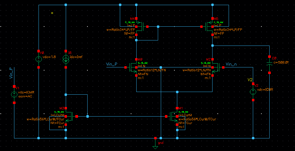
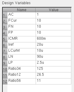
Hi,how to design signle stage OTA with the below specs in cadence 180nm technology.I have referred few book but I couldn't find any relevant info.Please help me with the step by step procedure.
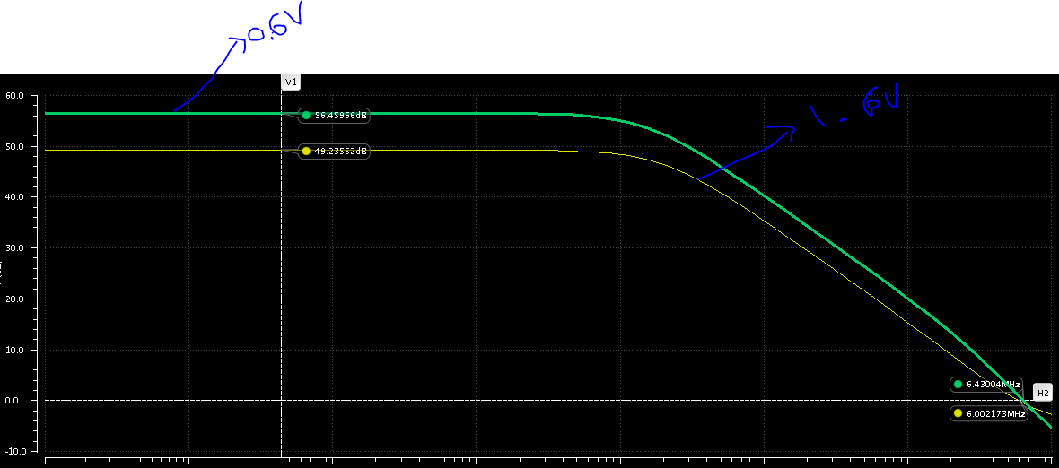
DC gain:min 52dB
Gain BW product: min 6MHz
large signal cutoff frequency :min 6Khz
output common mode:typical value -1.2v
input common mode range CMRi: min 0.6v and max 1.6v
load capacitance :typical 0.5 pf
supply voltage :1.8v

with all transistors minimum area.
 

Sorry its 1.2v .Output common mode VCMo: typical value 1.2v
 

For single stage OTA your start point should be:

Gain= gm.ro

UGB= 1/[(2*pi)*(ro*CL)] x gm.ro = gm/(2*pi*CL)

So your UGB is 6MHz you have your Cl you can find gm

once you have gm, it is equal to gm of first stage Gm=gm1

gm=2Id/Vov you may set vov = 0.2 so you can find Id and then W/L

in order to set the gain:

Gain =gm.ro = gm1*ro (not very precise)

what is ro ( Rup (PMOS) || Rdown (NMOS))

If we want to have rough estimation:

Gain = gm1.ro = [2Id/(Vov)] * [(Va*L)/Id] = (2 * Va * L)/Vov

For increasing gain for exmaple:

1) Decrease Vov of transistors (it means that if you want to have previous gm, you have to re-calculate W/L for new Vov)

2) Increase L of last stage.
 

This may help you

ota1.png
 
  • Like
Reactions: e0e0

    e0e0

    Points: 2
    Helpful Answer Positive Rating
Thanks Ata_sa16 and erikl.
I designed this circuit with N differential pair.


and i chose design parameters like this


but I am not meeting specs with 1.6V


could someone tell me how to increase gain at 1.6v

Thanks alot
 

I don't know which Vth values your models have. With my models (Vth values s. image) and the current and W/L values shown, the schematic works well with gain=60dB over ICMR = 0.6 .. 1.6V:
180nm_1-stage-OTA-immadi.png

Here's a transient simulation plot with stimulation of f=10kHz and V1ac=0.1mV , for ICMR = 0.6 , 1.1 & 1.6V :
Simulation with V1ac=0.1mV.png
 

In my tool,

Vth for nmos=0.4v
Vth for Pmos=-0.5v

So with your W and L values, I obviously didn't meet my specs. I got around 30 dB and 4MHz GBW
 

please explain type of OTA(folded cascode ,teliscop etc. ) design tool etc.
all transistor are biased in such a way that they must be in saturation state for all input/output voltage swing.
if you design folded cascode OTA input stage need large current to improve trans-conductance and output cascode branches need lower current to increase load resistance.
in virtuoso use view-> show operating point
 

Status
Not open for further replies.

Part and Inventory Search

Welcome to EDABoard.com

Sponsor

Back
Top