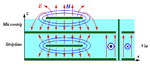
We can also analyze it in terms of E/H fields .

As illustrated above, both microstrip line and stripline radiate E-field outside.
Thus, we need ground plane to absorb their E fields.
And larger the ground plane,
lower the ground impedance, more the E-fields that ground plane absorbs.
If ground plane is not large enough, both microstrip and stripline have EMI emission risk.

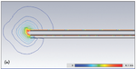
Besides, some PCB layout guides tell you that don’t lay your PCB layout trace
(especially high speed digital signal , or power trace) in the board edge.
It’s the reason as well. Otherwise, there will be Fringing Effect.

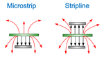
As illustrated above, both microstrip line and stripline radiate E-field outside.
Thus, we need ground plane to absorb their E fields.
And larger the ground plane,
lower the ground impedance, more the E-fields that ground plane absorbs.
If ground plane is not large enough, both microstrip and stripline have EMI emission risk.
Besides, some PCB layout guides tell you that don’t lay your PCB layout trace
(especially high speed digital signal , or power trace) in the board edge.
It’s the reason as well. Otherwise, there will be Fringing Effect.