Continue to Site

Welcome to EDAboard.com

Welcome to our site! EDAboard.com is an international Electronics Discussion Forum focused on EDA software, circuits, schematics, books, theory, papers, asic, pld, 8051, DSP, Network, RF, Analog Design, PCB, Service Manuals... and a whole lot more! To participate you need to register. Registration is free. Click here to register now.

[PIC] Zero Crossing Detector with pic 12F1822

Status
Not open for further replies.

Amanda Lima

Junior Member level 1
Joined
Jul 24, 2021
Messages
16
Helped
0
Reputation
0
Reaction score
0
Trophy points
1
Activity points
111
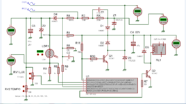
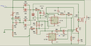
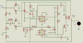
Hi, from what I understand zero crossing is normally used for smooth actuation of loads, increasing their service life. Someone has already made a circuit with pic that allows you to identify the moment when the AC mains voltage crosses the zero volt line. I need to connect a relay and I don't know how to make the code, I will not use amplifiers, optocouplers. The circuit is now ready, only pin 4 (RA3) of pic 12f1822 will be used, this is the photocell schematic, a correction, trimpot RV1 and RV2 is 100k, capacitor C2 is 5nF and zener diode Z1 24 volts, Z3 56 volts Z2 5 volts.
Code:
#include <main.h>
//;;;;;;;;;;;;;;;;;;;;;;;;;;;;;;;;;;;;;;;;;;;;;;;;;;;;;;;;;;;;;;;;;;;;;;;;;;;;


//int16 minuto = 0;
            
#fuses NOMCLR INTRC_IO PLL_SW
#device ADC = 10

#use delay(clock=32000000)
//#use fast_io(a)
//int32 cnt = 0;

#INT_TIMER1
void  TIMER1_isr(void)
{
clear_interrupt(int_timer1);
set_timer1(15536); // 0,05 segundo para  32MHZ
//set_timer1(3036); // 0,5 segundo para  4MHZ
              //cnt++;
//if(contador==1)

//output_toggle(pin_a5);
//min++;   //;;;;;;;;;;;;;;;;;;;;;;;;;;;
//contador = 0;


//contador++;
//set_timer1(15536); // 0,05 segundo para  32MHZ
//set_timer1(3036); // 0,5 segundo para  4MHZ
//clear_interrupt(int_timer1);

}


void main()
{
     setup_adc_ports(sAN1|sAN2|sAN3);
     setup_adc(ADC_CLOCK_INTERNAL);
     setup_timer_1(T1_INTERNAL|T1_DIV_BY_8);      //524 ms overflow
     set_timer1(15536);    // 0,05 segundo para  32MHZ
     //set_timer1(3036);  // 0,5 segundo para  4MHZ
     setup_oscillator(OSC_8MHZ | OSC_PLL_ON);   // Set internal oscillator to 32MHz (8MHz and PLL)
    // set_tris_a  (0b00011110 );   //(0b00011110);      // HEX 1E  RA Tris  76543210  0X1E
    //set_tris_a  (0x1E);
     clear_interrupt(int_timer1);
     enable_interrupts(INT_TIMER1);
     enable_interrupts(GLOBAL);
     output_high(pin_a0);
     output_low(pin_a5);


 while(TRUE){
 
 if (!input(pin_a3) )
 {
 output_high(pin_a5);
//output_toggle(pin_a5);
}
 else
  {
  output_low (pin_a5);
  }
   }
    }
 
 
  /* {
    
    if (cnt >= 1200 )       //passou 1 minuto                   
    {
      cnt = 0;
      minuto++;
    }
 if (!input(pin_a3) ) && (minuto < 10) 
 {
 output_high(pin_a5);

 }
 
   if (!input(pin_a3) ) && (minuto >= 10)                     
{
 output_low(pin_a5);

 }
 
  if(minuto >= 20)
{
 
minuto = 0;
 } 
 
  }
   }


   */
 

Attachments

  • Esquema.png
    Esquema.png
    98.2 KB · Views: 252

Hi,

Please give matching informations. If the schematic is not correct, then correct the schematic.
Otherwise it just causes confusions, when one refers to the schematic and the other refers to the text.

To me the schematic as well as the text is confusing.

Please add some informations to the schematic. I have no idea about voltages, what is AC, what is DC, what is a power supply, what is analog what is digital, what is input what is output. What is valid, what is invalid?

Someone has already made a circuit with pic that allows you to identify the moment when the AC mains voltage crosses the zero volt line.
Is it the given schematic? Which node?
I need to connect a relay and I don't know how to make the code,
There already is a relay. Can or do you want to use it?
There already is code. Your code? Which lines do you want to keep or modify? Why, how?

I will not use amplifiers, optocouplers.
What does that mean? There are no such devices...
The circuit is now ready, only pin 4 (RA3) of pic 12f1822 will be used, this is the photocell schematic, a correction, trimpot RV1 and RV2 is 100k, capacitor C2 is 5nF and zener diode Z1 24 volts, Z3 56 volts Z2 5 volts.
No idea what you want to tell.

****
Generally switching ON some load at zero cross reduces EMI.
On the other hand one does not want to switch ON inductive loads like transformers at zero cross, because this causes high inrush current due to core saturation.
So whether switching ON at zero cross makes sense or not depends on the load.
But "the load" something unknown ...

Is the load connected to the relay contacts?
If so, then zero cross switching makes no sense at all, because there is a lot of time delay between activating the relay coil and closing the relay contact.
The time is not very precise and varies with time, remanence, aging.. also contact bouncing will cause multiple "close and open" of the cintact.

Klaus
 

Your code seems to have most of the useful bits comments out so it is hard to understand what it is really gtrying to do.
My guess is that you are setting up a timer and useing the interrupt to increment the 'cnt' variable in the ISR. That variable is then checked in the main loop to see when a minute has elapsed.
Whenever a variable is written in an ISR and read outside it, the variable MUST be declared 'volatile'. Doing so tells the compiler that its value can be changed when the compiler is not aware of it and so will ALWAYS read the value from the varable location rather than trying to cache it in a register somewhere. It is quite legitimate for the compiler to cache a variable's value in a register (even without any optimisation), especially if the variabel is being read frequently. If it does this and is not told that the variable value can be updated esewhere (e.g. in the ISR) then it will always assume that the cached value is the right one as it thinks it has complete control over the variable value. Declaring the variable 'volatile' tells the compiler that this assumption cannot be made mand to ALWAYS read the value from the variable location.
Susan
 

Hi,

Please give matching informations. If the schematic is not correct, then correct the schematic.
Otherwise it just causes confusions, when one refers to the schematic and the other refers to the text.

To me the schematic as well as the text is confusing.

Please add some informations to the schematic. I have no idea about voltages, what is AC, what is DC, what is a power supply, what is analog what is digital, what is input what is output. What is valid, what is invalid?


Is it the given schematic? Which node?

There already is a relay. Can or do you want to use it?
There already is code. Your code? Which lines do you want to keep or modify? Why, how?


What does that mean? There are no such devices...

No idea what you want to tell.

****
Generally switching ON some load at zero cross reduces EMI.
On the other hand one does not want to switch ON inductive loads like transformers at zero cross, because this causes high inrush current due to core saturation.
So whether switching ON at zero cross makes sense or not depends on the load.
But "the load" something unknown ...

Is the load connected to the relay contacts?
If so, then zero cross switching makes no sense at all, because there is a lot of time delay between activating the relay coil and closing the relay contact.
The time is not very precise and varies with time, remanence, aging.. also contact bouncing will cause multiple "close and open" of the cintact.

Klaus
Hi, there are some faulty photocells that have fallen into my hands. The scheme posted so far has been fixed by a colleague because mine was a mess, I will post my scheme and waveforms and code used in the tests, enabling port_A_pullups(0x08) ; had a change in the waveform, remembering that this photocell turns on near the zero of the network. A part of the code was placed just for testing RA3 the rest is incomplete it is valid and I will use putting RA3 to detect crossing zero, this relay already exists in the circuit, the load will be connected to the relay contacts. About this “zero cross-switching does not make sense, because there is a long time delay between the activation of the relay coil and the closing of the relay contact. Time is not very precise and varies with time, remanence, aging”. Was it the fault of the one who designed the circuit? Or who did think about it? About this “also the oscillation of the contact will cause multiple "closes and opens" of the contact. ” The relay will turn on close to the mains zero and will turn off after a programmed time, at the moment I am focused on turning on the relay.
Code:
#include <main.h>
//;;;;;;;;;;;;;;;;;;;;;;;;;;;;;;;;;;;;;;;;;;;;;;;;;;;;;;;;;;;;;;;;;;;;;;;;;;;;


//int16 minuto = 0;
            
#fuses NOMCLR INTRC_IO PLL_SW
#device ADC = 10

#use delay(clock=32000000)
//#use fast_io(a)
//int32 cnt = 0;

#INT_TIMER1
void  TIMER1_isr(void)
{
clear_interrupt(int_timer1);
set_timer1(15536); // 0,05 segundo para  32MHZ
//set_timer1(3036); // 0,5 segundo para  4MHZ
              //cnt++;
//if(contador==1)

//output_toggle(pin_a5);
//min++;   //;;;;;;;;;;;;;;;;;;;;;;;;;;;
//contador = 0;


//contador++;
//set_timer1(15536); // 0,05 segundo para  32MHZ
//set_timer1(3036); // 0,5 segundo para  4MHZ
//clear_interrupt(int_timer1);

}


void main()
{
     port_A_pullups(0x08);
     setup_adc_ports(sAN1|sAN2|sAN3);
     setup_adc(ADC_CLOCK_INTERNAL);
     setup_timer_1(T1_INTERNAL|T1_DIV_BY_8);      //524 ms overflow
     set_timer1(15536);    // 0,05 segundo para  32MHZ
     //set_timer1(3036);  // 0,5 segundo para  4MHZ
     setup_oscillator(OSC_8MHZ | OSC_PLL_ON);   // Set internal oscillator to 32MHz (8MHz and PLL)
    // set_tris_a  (0b00011110 );   //(0b00011110);      // HEX 1E  RA Tris  76543210  0X1E
    //set_tris_a  (0x1E);
     clear_interrupt(int_timer1);
     enable_interrupts(INT_TIMER1);
     enable_interrupts(GLOBAL);
     output_high(pin_a0);
     output_low(pin_a5);


 while(TRUE){
 
 if (!input(pin_a3) )           // test
 {                              //
                                
   output_high(pin_a5);
 
//output_toggle(pin_a5);
}
 else
  {
  output_low (pin_a5);
  }
   }
    }                            //test
 
 
  /* {
    
    if (cnt >= 1200 )       //passou 1 minuto                   
    {
      cnt = 0;
      minuto++;
    }
 if (!input(pin_a3) ) && (minuto < 10) 
 {
 output_high(pin_a5);

 }
 
   if (!input(pin_a3) ) && (minuto >= 10)                     
{
 output_low(pin_a5);

 }
 
  if(minuto >= 20)
{
 
minuto = 0;
 } 
 
  }
   }


   */
Fotocélula..PNG
Esquema..PNG
 

Hi,

sadly the schematic is more messy than before. I don´t want to go deeper through it.
* GND and supply symbols are for free ;-) So use them to aviod big, confusing GND and supply nets.
* Junction dots are a chaos here.

If you expect to switch the load (connected at the relay contacts) at zero cross: then better forget the idea. The relay gives about 15ms from givign voltage to the relay coil until the contact switches.
The 15ms do vary widely from item to item, with temperature, with aging, with remanence....
15ms! Mind: it´s just 5ms from zero cross to peak of a 50Hz sine.

If you want to learn, then try it.
If you want to be successful you have to replace the slow relay with a fast semiconductor.

I´m not sure if there ever was the idea of the designer to switch ON the load at zero cross.

Klaus
 

sadly the schematic is more messy than before. I don´t want to go deeper through it.
* GND and supply symbols are for free ;-) So use them to aviod big, confusing GND and supply nets.
* Junction dots are a chaos here.

If you expect to switch the load (connected at the relay contacts) at zero cross: then better forget the idea. The relay gives about 15ms from givign voltage to the relay coil until the contact switches.
The 15ms do vary widely from item to item, with temperature, with aging, with remanence....
15ms! Mind: it´s just 5ms from zero cross to peak of a 50Hz sine.

If you want to learn, then try it.
If you want to be successful you have to replace the slow relay with a fast semiconductor.

I´m not sure if there ever was the idea of the designer to switch ON the load at zero cross.
As mentioned the load connected to the relay contacts when commuting across zero does not make sense, as there is a long delay time between activation of the relay coil and closing of the relay contact.
The time is not very precise and varies with time, remanence, aging, but I see a circuit using a relay and I don't understand, as an example of a circuit that uses a CD 4013 IC that I'm going to post, with the words "Exclusive switching system nearby to zero of the network (sinenoid) increasing the useful life of the load and the relay,” whoever works with electricity has already had the opportunity to see several photocells of this type.
 

Attachments

  • Fotocélula SP.PNG
    Fotocélula SP.PNG
    56 KB · Views: 150

Hi,

The schematics become more even more messy.
* shorted R1 and R2
* zeners in a rectifier circuit
* ridiculous capacitor value 8uF, 9uF
* BJT driven without base resistor
* a lot of junction dot mistakes
* no clear power supply, no supply symbols
* very messy GND wiring without symbols
* ignoring all schematuc drawing standards

... the schematic is almost unreadable

If you can do now, I bet you can't do in half a year

Just for me speaking:
I'm leaving this thread, because it's very likely that I make a lot of errors by not understanding the schematic and it's function and your textual descriptions.

I recommend to learn at least some basics in drawing schematics...no need to be perfect.
Maybe you have a workmate, friend, neighbour ... to assist you with this.
There are also a lot of tutorial videos in the internet.

Good luck with your project

Klaus
There was a short on R1 in the previous scheme because it was being tested at 24 volts, I will post the new scheme corrected and there is no resistor at the base of Q1 in the posted scheme because it is an A8C code transistor with a 47k resistor integrated in its base and another in base and emitter of 47k.
 

Attachments

  • Fotocélula SP..PNG
    Fotocélula SP..PNG
    48.2 KB · Views: 150

Status
Not open for further replies.

Part and Inventory Search

Welcome to EDABoard.com

Sponsor

Back
Top