cupoftea
Advanced Member level 5
Hi,
Will the micro be damaged by the (non series resistor protected) opamp input?
LTspice and jpeg attached.
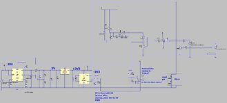
The micro has a -3v3 rail, and a 20V rail.
Micro has rail +3v3 to 0V.
Its a TL084C opamp.
What would be the worst circumstance for the micro?
The opamp output current is clamped to some 26mA, as you know,
Maybe micro can stand a short blast at 26mA?
TL084C opamp
STM32F103V micro (100pin)
The opamp goes into pin 35 of the micro which is labelled as an Analog input. ("PB0/ ADC_IN8 /T3_C3")

Will the micro be damaged by the (non series resistor protected) opamp input?
LTspice and jpeg attached.
The micro has a -3v3 rail, and a 20V rail.
Micro has rail +3v3 to 0V.
Its a TL084C opamp.
What would be the worst circumstance for the micro?
The opamp output current is clamped to some 26mA, as you know,
Maybe micro can stand a short blast at 26mA?
TL084C opamp
TL084 data sheet, product information and support | TI.com
TI’s TL084 is a Quad, 30-V, 3-MHz, 13-V/µs slew rate, In to V+, JFET-input op amp. Find parameters, ordering and quality information
www.ti.com
STM32F103V micro (100pin)
The opamp goes into pin 35 of the micro which is labelled as an Analog input. ("PB0/ ADC_IN8 /T3_C3")
Attachments
Last edited: