Continue to Site

Welcome to EDAboard.com

Welcome to our site! EDAboard.com is an international Electronics Discussion Forum focused on EDA software, circuits, schematics, books, theory, papers, asic, pld, 8051, DSP, Network, RF, Analog Design, PCB, Service Manuals... and a whole lot more! To participate you need to register. Registration is free. Click here to register now.

Why Transmission gate in FlipFLops

Status
Not open for further replies.

Prashanthanilm

Full Member level 5
Joined
Aug 24, 2012
Messages
302
Helped
36
Reputation
72
Reaction score
36
Trophy points
1,308
Activity points
2,950
Hi,

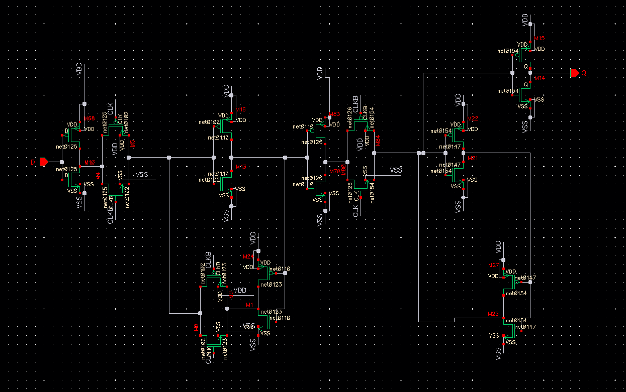
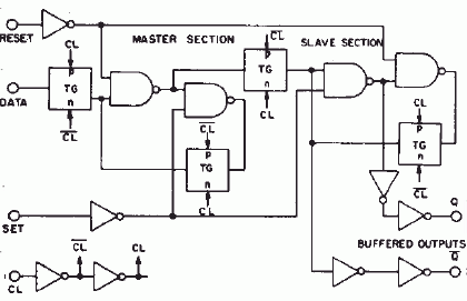
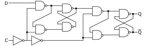
What is the need of transmission gate in FF?

I mean rather than clock signal (transparent and non-transparent).

What if I don't put TG in my feedback circuit. How it will effect my schematics performance?

Thank you,
Prashanth
 

Hi Prashant,
The tx gate in feedback path is essential as it prevents output from floating. Just visualize, When clk=0(or 1), input pass transistor is ON and o/p gets input value but when clk=1(or 0), if tx gate in feedback path(which will be ON) was not there, output would have floated.

It affects schematic performance as if output floats for a long time, it can be disturbed by leakage coming at output node.
 

Hi Prashant,
output would have floated.

It affects schematic performance as if output floats for a long time, it can be disturbed by leakage coming at output node.

Why will be the output be floating?
The back to back inverters in the feedback will have the strength to take the output node to VDD and VSS..

Ok. For more clarification I have attached the schematic below:


Hi. The basic storage element in static Flip Flop is a pair of back to back connected inverters. If the inverters are named A and B, you have two nodes in the circuit o/p of A and o/p of B. A = !B

'A' can be zero or one based upon the noise in the circuit at power up.
You need some kind of mechanism to break this positive feedback loop of the 2 inverters and feed in a new value.
The transmission gate allows you break this loop and feed in a new value.

Hope this helps...
 

Before discussing about implementation techniques, you should become clear about the inteded function of said D-FF.

The usual transfer gate is strictly spoken a master–slave edge-triggered D flip-flop, see https://en.wikipedia.org/wiki/Flip-...ster.E2.80.93slave_edge-triggered_D_flip-flop

Transfer gate is the preferred implementation in CMOS technlogy, because it involves least transistor count and best timing performance. But the same function can be also achievd with regular logic gates. You'll find this implementation in TTL logic where no transfer gates are available. Shown below without the additional asynchronous set/reset present in the CMOS circuit (from CD4013 datasheet).

5731691000_1362304890.gif


500px-D-Type_Flip-flop_Diagram.svg.png
 

Hi.
You need some kind of mechanism to break this positive feedback loop of the 2 inverters and feed in a new value.
Hope this helps...

I understood a bit, But can you tell why we want to break loop and feed a new value?

What will happen if the loop is not breaken?

- - - Updated - - -

Transfer gate is the preferred implementation in CMOS technlogy, because it involves least transistor count and best timing performance. But the same function can be also achievd with regular logic gates. You'll find this implementation in TTL logic where no transfer gates are available. Shown below without the additional asynchronous set/reset present in the CMOS circuit (from CD4013 datasheet).

Transmission gate involves less transistor circuit and best timing performance.
That was Helpful.

Even there are many ways to achieve FF using logic gates as you mentioned above,Thanks for the diagram.

But , Here the question is something else.

I have attached the schematic in my previous post, I want to know more about the behavior of the circuit , if there is not TG in FB.
Hope it makes sense now.
 

Status
Not open for further replies.

Part and Inventory Search

Welcome to EDABoard.com

Sponsor

Back
Top