allennlowaton
Full Member level 5
This does not make much sense. At what value of vdd are you running ac analysis?
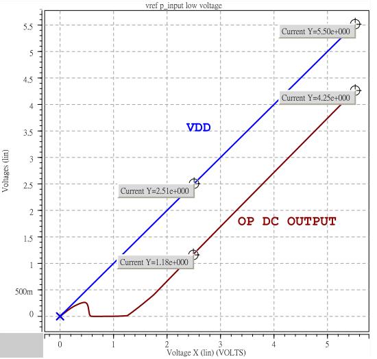
The Vdd I used for the AC is a ramp: vdd vdd gnd pwl(0s 2.7v, 5m 5.5V,R)
Follow along with the video below to see how to install our site as a web app on your home screen.
Note: This feature may not be available in some browsers.
This does not make much sense. At what value of vdd are you running ac analysis?
the AC analysis will run only at one specific DC point, not sure which one it will pick in this case (I guess the first). Please try to run AC with vdd at one single value e.g. 2.7V
Hi allennlowaton,
may I ask you if you know what you are doing - and why?
There are several forum members who are trying to help you.
Why don't you follow their recommendations?
* You are doing an ac analysis by sweeping the power supply? What do you expect by doing this?
* For stability analyses you need the loop gain. Why don't you show us this gain? In one of your graphs there was only the voltage at one node (instead the ratio of two node voltages); the same for the phase response.
* The last graph shows a curve designated as "gain" - however the axis is named as a current: "result I(in)" . Confusing!
* Something is wrong since the gain curve does not cross the frequency axis.
* Therefore, you have been asked to simulate the bias point. No answer!
* It was recommended to start simulations at lower frequencies. No response.
__________________
It's really not easy to help you.
LvW
")
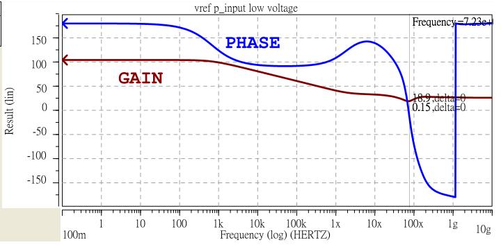
This is the AC simulation result using Vdd = 2.7V.
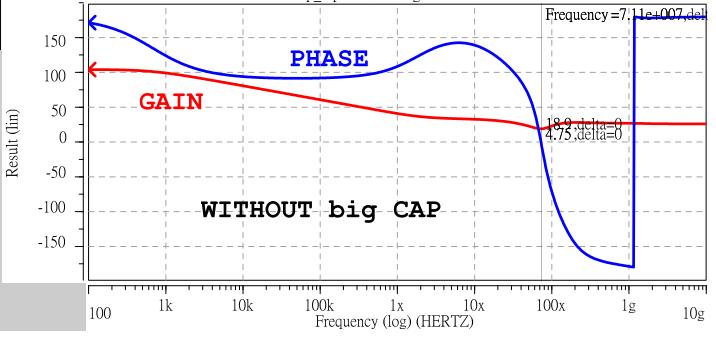
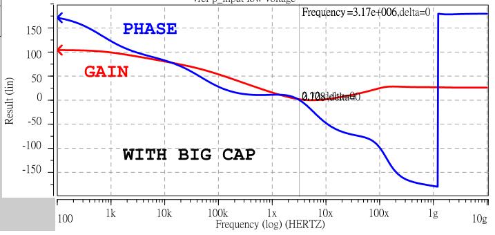
At zero crossing of the phase, the gain is greatly reduced from ~19dB(without big cap) to ~2dB(with big cap)....
Pls post your schematic of OPb. I recommend single-stage opamp (like current mirror OTA. cascode can be added for higher gain).
More stages will introduce more poles and it makes stability worse usually. Generally, every stage will contribute one pole.
For stability, the loop is compensated to a one pole system that will be stable. So first, it is better to reduce pole number.
Then generate zero to compensate high frequency zero and leave the lowest pole as the dominate pole.