Continue to Site

Welcome to EDAboard.com

Welcome to our site! EDAboard.com is an international Electronics Discussion Forum focused on EDA software, circuits, schematics, books, theory, papers, asic, pld, 8051, DSP, Network, RF, Analog Design, PCB, Service Manuals... and a whole lot more! To participate you need to register. Registration is free. Click here to register now.

why does latch up occur only in CMOS technology?

Status
Not open for further replies.

Krishh

Newbie
Joined
Jun 22, 2011
Messages
3
Helped
0
Reputation
0
Reaction score
0
Trophy points
1,281
Activity points
1,346
why does latch up occur only in CMOS technology? Is there any possibilities of Latch up in other than CMOS technology..? i.e. in NMOS, PMOS alone.. or cobination of those..
 

A byproduct of the Bulk CMOS structure is a pair of parasitic bipolar transistors. The collector of each BJT is connected to the base of the other transistor in a positive feedback structure. A phenomenon called latchup can occur when (1) both BJT's conduct, creating a low resistance path between Vdd and GND and (2) the product of the gains of the two transistors in the feedback loop, b1 x b2, is greater than one. The result of latchup is at the minimum a circuit malfunction, and in the worst case, the destruction of the device.

image6.gif image7.gif

This parasitic pair of bipolar transistors is not formed in NMOS or PMOS alone. So there is no latchup problem in NMOS or PMOS.
 
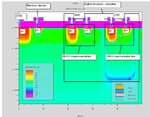
la.jpg
in this fig minimum connections required for latch up are shown.. The arrow (white colored) near p+ to n+ is the electron path. If .7 volts drop in that region below source, it will trigger latch up.. Hence what i wanna ask, is there any other possibility where this NPNP structure will form? (other than CMOS tech) or any body come across latch up problems in other than CMOS tech?? viz. when diode placed near NMOS/PMOS some thing that kind..
 

Status
Not open for further replies.

Part and Inventory Search

Welcome to EDABoard.com

Sponsor

Back
Top