Continue to Site

Welcome to EDAboard.com

Welcome to our site! EDAboard.com is an international Electronics Discussion Forum focused on EDA software, circuits, schematics, books, theory, papers, asic, pld, 8051, DSP, Network, RF, Analog Design, PCB, Service Manuals... and a whole lot more! To participate you need to register. Registration is free. Click here to register now.

where will core and prepreg use ?

Status
Not open for further replies.

kabaleevisu

Advanced Member level 2
Joined
Apr 14, 2010
Messages
616
Helped
85
Reputation
170
Reaction score
81
Trophy points
1,308
Location
Chennai,India
Activity points
4,512
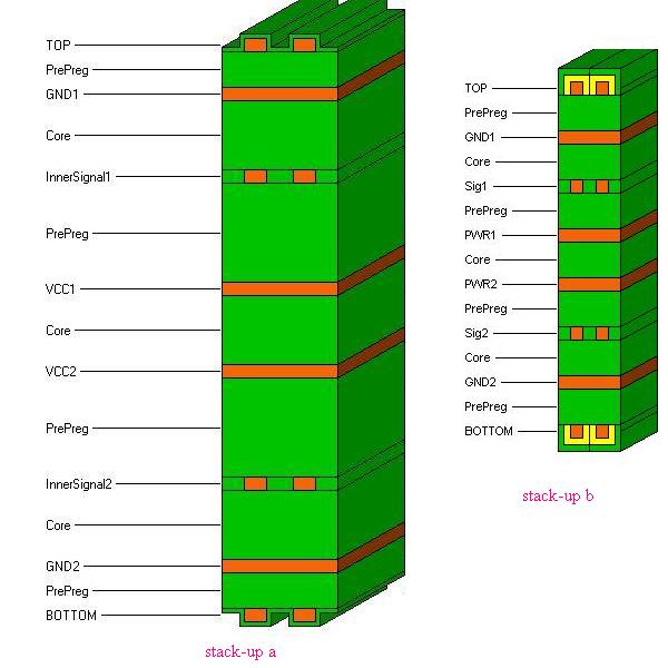
where will core and prepreg can be used in this stack-up ?

Hi everyone,

in my design has BGA(256pins),DC-DC converter,opto isolator,schmitt trigger,connector is avaiable and power and ground are
1.5V(1.5A),3.3V(2A),5V(1A),+15V_FTR,+15V_DC,5VDC,+ 5V_FTR,+24V_ISO,ISO_GND,GND,AGND,minimum pitch details for package
tssop package-0.65mm,soic-1.27mm,BGA Pitch-1mm

i am planning to design in 6 layer ,Here i like to choose any one

---------------- mounding pads/low freq signal
---------------- Ground
---------------- Hig freq signal
---------------- High freq signal
---------------- power
---------------- Low freq signal
stack -up (a)

---------------- sig(Hi)
---------------- Gnd
---------------- sig(v1)
---------------- sig(H2)
---------------- PWR
---------------- SIg(v2)
stack -up (b)

----------------GND/Mounding PADS
----------------SIG
----------------GND
----------------PWR
----------------SIG
----------------GND
stack -up (c)


i have some queries in my stack-up design
1) where core and preperg will come ?
2) which stack-up is best amoung three ?? why ?? what is horiantal and vertical routing?? what is the use of it ??
3) which dielectrical meterial is used commenly ??
 
Last edited:

I am not answering about the prepreg as I am not a pcb designer. I am commenting on your stackup after looking at your few choices. I would put the split power plane between two ground plane in the middle. Let the two ground sandwich the split power plane. Then you have 3 layers of signal traces. on the outer layer.

My suggestion is

Top-------------components/signal/ fill copper ground as needed.
Inner1-----------GND1 continuous.
Inner2----------Split power planes
Inner3----------GND2 continuous.
Inner4----------Signals.
Bottom---------Signals.

There is no difference where to put what signals, worry more about the trace impedance ( microstrip) than anything else. Don't let the digital signal traces cross the analog portion. Another thing is you need to put the plane in more symmetrical stackup, don't put more plane on the top or the bottom, it will cause the board to warp. You can play with the dielectric thickness of my stackup so the two ground plane is close to the center of the board.

I explained in detail the reason behind all these:

https://www.edaboard.com/threads/273075/
 

hi,

thanks for your reply ,but for your stack-up has not reference plane for bottom layer inner3 and inner4 need to interchange right...
 

hi,

thanks for your reply ,but for your stack-up has not reference plane for bottom layer inner3 and inner4 need to interchange right...

I read your current requirement. If you can get all the signals into the top and bottom layers, you can do this:

Top-----------Signal/components
Inner1--------GND1
Inner2--------Split power plane.
Inner3--------Split Power, ISO 24V and ISO 24V ground.
Inner4--------GND2
Bottom--------Signal.

I really never have to use 3 signal layers, it should not be a problem as you put all the split power and heavy current stuff in the middle isolate by the two ground plane.

Or just follow my original stack up You can have both bottom and Inner 4 reference to ground plane of Inner 3. You should have the stackup so the dielectric is thinner between bottom and Inner 4, Inner 4 to Inner3. Make sure you try to run traces of bottom run perpendicular to Inner4 so their interaction is minimal. Put the ISO 24 ground as thick signal trace in Inner4.

In the other post, I talked about how the ground image return current concentrate right under the signal trace, so you can predict the interaction of the signal traces. Sensitive signal traces should not run in parallel for long distance with another noisy trace. Avoid cutting ground plane unless the engineer tell you to do it, then it's the engineer's responsibility, not yours.

I used this stackup for quite a few 6 layer board that had high speed mixed signal circuits, never had any problem. Read my explanation why cutting ground plane is a very bad idea unless you really know what you are doing. That a single continuous ground plane works as long as you take into consideration of the image return current concentration within a few trace width under the trace.

You need to have ground vias at regular intervals like 1" spacing to stitch the GND1 and GND 2 together for high frequency components. This is particular important in part that has a lot of signal traces going from top to bottom. The vias serve to give a path for the image current to jump from one surface to the other. Remember RF current run on the surface of the ground plane.
 
Last edited:

Hi everyone,
i have some doubt in stack-up design,here i mention two
stack-up stack-up (a) and stack-up (b)

why core is between inner and ground layer in stack-up (a)
instand of this if i use prepreg what will happen in this board


core is hard material so we need to use the core in center of
stack-up right but in the stack-up prepreg is center
why ??so please explan any one


Status
Not open for further replies.

Part and Inventory Search

Welcome to EDABoard.com

Sponsor

Back
Top