Continue to Site

Welcome to EDAboard.com

Welcome to our site! EDAboard.com is an international Electronics Discussion Forum focused on EDA software, circuits, schematics, books, theory, papers, asic, pld, 8051, DSP, Network, RF, Analog Design, PCB, Service Manuals... and a whole lot more! To participate you need to register. Registration is free. Click here to register now.

Where to put current sense resistor in Boost PFC?

Status
Not open for further replies.

cupoftea

Advanced Member level 5
Joined
Jun 13, 2021
Messages
2,609
Helped
54
Reputation
108
Reaction score
115
Trophy points
63
Activity points
13,682
Hi,
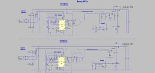
Which of the Boost PFC schems is best? One has the current sense resistor near the controller, and the other has the current sense resistor near the current sense transformer output. There is a decent ground plane under all of it.

Which is best, top or bottom schem?

LTspice sim and jpeg schem attached.

UCC28070A PFC controller datasheet
 

Attachments

  • Boost PFCs comparison.zip
    4.9 KB · Views: 96
  • Boost PFCs comparison.jpg
    Boost PFCs comparison.jpg
    197.2 KB · Views: 115

If you split your CT burden resistor (increase value by 2 & then parallel them at 2 different locations) & put one close to CT & the other one close to controller will give you better noise immunity, also there should be separate return track just below the positive CS track in the layout to prevent any impedance mismatch / noise
 
Thanks yes, that sounds good advice, at the moment, the burden res is at the CST....because putting the burden at the controller would have meant also routing the ramp signal back there aswell....i hope we dont get issues...we do have a light rc filter at the controller.

Do you think we will get noise problems?

I didnt want to route the burden res and ramp sig back, as it will eventually be a 4 phase PFC, and routing all that lot back to the controller will take up quite some room, and complicate the layout.
 
Last edited:

Between the two options I'd go for putting the burden resistor close to the CT. But I would also implement a star GND for the current sense transformer and burden resistor which connects to GND only near the pwm controller. Still two traces instead of one, but that's likely the only way to mitigate ground bounce.
 
Thanks yes, that sounds good advice, at the moment, the burden res is at the CST....because putting the burden at the controller would have meant also routing the ramp signal back there aswell....i hope we dont get issues...we do have a light rc filter at the controller.

Do you think we will get noise problems?

I didnt want to route the burden res and ramp sig back, as it will eventually be a 4 phase PFC, and routing all that lot back to the controller will take up quite some room, and complicate the layout.
If you lay your CT tracks one over other (no other switching track should overlap or cross these tracks) you can use one burden resistor near controller & feed slop comp ramp into it.
 
Status
Not open for further replies.

Similar threads

Part and Inventory Search

Welcome to EDABoard.com

Sponsor

Back
Top