ccarrot
Newbie level 6
Hi all:
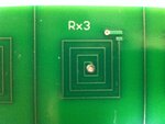
I'm a totally new in designing and fabricating PCB. I've made a very simple PCB on which there is just one Surface Mounted Device resistor on the upper-right corner (see the first picture), but when the PCB's back, the place where the resistor should be mounted is covered by the green silk ----- isn't there some like silver-color Pad on the squared area? cuz the resistor package is covered, the resistor can't be mounted there, then
1, what should I do now?
2, What mistake did I make when I drew this board?
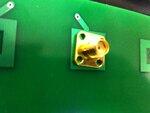
3, If I want to put a large area of a Pad on the board in order to mount a SMA connector, how can I do then? (see the second picture, I've put a large area of GND on the bottom side, but it is covered by the green too ---- no copper on it to be used to mount)
Thank you very much for any help!

