thanhFF
Junior Member level 2
Hi all,
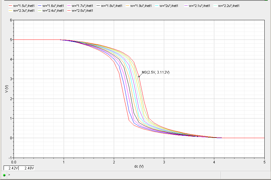
I am doing a parametric analysis on an inverter by using Spectre. The PDK used is GPDK045 from Cadence.
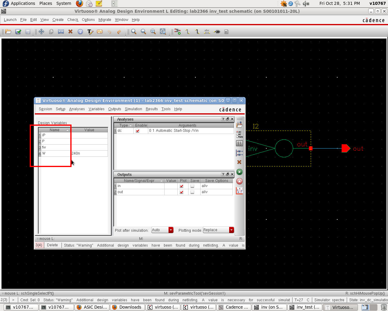
The circuit and setting are shown in tha t


 .
.
My question is beside W(The Width of PMOS), what are other 3 variables(fw, P, iP) come from? What are they? When I point at them and select Find, it said not in the schematic, just only W can be found.
I tried the same method for inverter made from NCSU AMI 0.6. Everything worked fine, so wondering why MOSs from GPDK045 have some unknown variables?
Anyone has anything ideas?
Thanks
These are 4 pics included
1. Schematic
2. Test bench
3. Parametric Analysis Setup
4. 4 Variables on the left, 3 unknown
Also have log file after run Spectre.
I am doing a parametric analysis on an inverter by using Spectre. The PDK used is GPDK045 from Cadence.
The circuit and setting are shown in tha t
.My question is beside W(The Width of PMOS), what are other 3 variables(fw, P, iP) come from? What are they? When I point at them and select Find, it said not in the schematic, just only W can be found.
I tried the same method for inverter made from NCSU AMI 0.6. Everything worked fine, so wondering why MOSs from GPDK045 have some unknown variables?
Anyone has anything ideas?
Thanks
These are 4 pics included
1. Schematic
2. Test bench
3. Parametric Analysis Setup
4. 4 Variables on the left, 3 unknown
Also have log file after run Spectre.
 .
.