Welcome to our site! EDAboard.com is an international Electronics Discussion Forum focused on EDA software, circuits, schematics, books, theory, papers, asic, pld, 8051, DSP, Network, RF, Analog Design, PCB, Service Manuals... and a whole lot more! To participate you need to register. Registration is free. Click here to register now.
Generally in LDO you have the pass transistor(PT) having a large cgs due to its large size. So, generally if you have opamp (in this case first opamp -->will have large output impedance) and if you load it directly with PT then you will get the pole releatievely at a very low frequency which wouldn't be too much sepeperated from the output pole (generally). So, buffer is used to seperate high resistive node from high capacitive node. So, inherently you dont need to reduce the bandwidth so much to achieve stability-->improves high freq PSRR. And as such I don't find the buffer to be useful, since it produces a lot more constraint on the swing, more current, etc. (One more thing to look at it is the buffer output looks like a inductor at some intermediate frequency & remember you have very high cap at the PT gate, so its boost the Q factor unless you burn a lot of current).
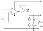
The 100% negative feedback of the buffer reduces the output impedance significantly to drive the gate transient capacitance to assert good load regulation.
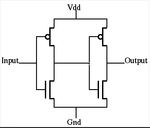
I designed the buffer by using two NOT gates as in the picture below.
The result is relatively good. PSRR is better at high frequency. However, as I was told, the buffer using two NOT gates is a digital not analog. How is it possible for LDO to work like that?
First of all not sure how did you see improvement in PSRR with this implementation. See the buffer shown in the first figure is totally analog and indeed it has to be. See, the buffer (can be five pack or folded cascode or anyother fancy structure) whose impedance is lowered to very low value by the feedback action.
This site uses cookies to help personalise content, tailor your experience and to keep you logged in if you register.
By continuing to use this site, you are consenting to our use of cookies.