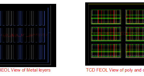
Continue to Site

Welcome to EDAboard.com

Welcome to our site! EDAboard.com is an international Electronics Discussion Forum focused on EDA software, circuits, schematics, books, theory, papers, asic, pld, 8051, DSP, Network, RF, Analog Design, PCB, Service Manuals... and a whole lot more! To participate you need to register. Registration is free. Click here to register now.

What is TCD cell in ASIC Physical Design?

Rashiba

Newbie
Joined
Oct 15, 2023
Messages
4
Helped
0
Reputation
0
Reaction score
0
Trophy points
1
Activity points
37
Hi everyone
I’m a beginner in Physical Design. While studying about Physical cells, I come accross TCD cell but have no glue about it. Could you explain what kind of that cell and its purpose?
Thank you
 
You mean like the old "CD Bars" we used to put on the
product die, along with the alignment marks and mask
level IDs, before smart people decided to put them in
the scribe lanes?

The ones in the link look a lot fancier and more of 'em.
Just what I would not want to sacrifice product die area,
for.

So I guess they're back on the product die, again. For
reasons. Somebody else's reasons.
It is a good reason actually. If you have an MPW, with designs of all sizes and shapes, you could potentially generate reticles that violate wafer-level rules. For instance, one rule from a know foundry is to have one TCD cell every 5mmx5mm region. The foundry then pushed these rules to individual dies, so if your tiny 1mmx1mm die respects the rule, you can make a reticle in any way you want and it will still be respected. Something like this.
 
It is a good reason actually. If you have an MPW, with designs of all sizes and shapes, you could potentially generate reticles that violate wafer-level rules. For instance, one rule from a know foundry is to have one TCD cell every 5mmx5mm region. The foundry then pushed these rules to individual dies, so if your tiny 1mmx1mm die respects the rule, you can make a reticle in any way you want and it will still be respected. Something like this.
I know that TCD cells are put on the die to monitor the critical dimension linewidth of some components when manufacturing. But I don’t understand the way TCD cell monitor the linewidth ?
 
I know that TCD cells are put on the die to monitor the critical dimension linewidth of some components when manufacturing. But I don’t understand the way TCD cell monitor the linewidth ?
the cell itself does nothing, it is not connected to anything. it is just process monitoring for the foundry
 

LaTeX Commands Quick-Menu:

Part and Inventory Search

Welcome to EDABoard.com

Sponsor

Back
Top