Continue to Site

Welcome to EDAboard.com

Welcome to our site! EDAboard.com is an international Electronics Discussion Forum focused on EDA software, circuits, schematics, books, theory, papers, asic, pld, 8051, DSP, Network, RF, Analog Design, PCB, Service Manuals... and a whole lot more! To participate you need to register. Registration is free. Click here to register now.

[SOLVED] what is operating gate voltage for n channel mosfet?

Status
Not open for further replies.

ishwaryasampath

Member level 1
Member level 1
Joined
Apr 25, 2013
Messages
37
Helped
0
Reputation
0
Reaction score
0
Trophy points
1,286
Visit site
Activity points
1,506
i was connected n channel mosfet (ZXMN6A08K) gate voltage as 5v and drain connected to 5v, the load connected at source. The problem was there was a voltage drop at the output ie., source. i want 5v output at the source. is there any solution to rectify this condition.
 

i was connected n channel mosfet (ZXMN6A08K) gate voltage as 5v and drain connected to 5v, the load connected at source. The problem was there was a voltage drop at the output ie., source. i want 5v output at the source. is there any solution to rectify this condition.
Only by changing the circuit. The DC output of a source follower is reduced by a voltage somewhat greater than the gate-source threshold voltage.

What is the purpose of the circuit?
 

source selection logic circuit

In this circuit 2nd p-channel MOSFET output voltage is dropped.We want to get drop less output(1.2v). Is there any solution for that ?

MOD:Threads merged, please don't cross post
 

Attachments

  • LOGIC CIRCUIT.pdf
    34.3 KB · Views: 156
  • Drawing2.pdf
    23.6 KB · Views: 133
Last edited by a moderator:

Re: source selection logic circuit

voltage of v1.2=1.2v

circuit is edited please refer the new attchment.
 

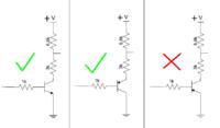
Then either the BC807 is upside down or it should be replaced with an NPN transistor.
 

Yes, that's the problem. The emitter is grounded and the collector is connected to a positive voltage. The emitter of a PNP transistor should have be at a more positive voltage than the collector.

 
Last edited:

i m tried that logic also. even 1.2 volt drop occur. there s nothing in that transistor switching.the problem is voltage drop occurs in second p channel output
 

The problem is with the NMOS transistor.

For a NMOS transistor with gate at Vdd and Drain at Vdd, the source can be at most Vdd-Vth, any higher than this voltage, and the NMOS would be in subthreshold, i.e. OFF.

This is why you see a voltage drop of 1.2V which is the Vth of the transistor.

You need to use a PMOS switch to pass Vdd or both NMOS and CMOS switch (i.e. a CMOS switch) of you need to pass both Gnd and Vdd.

A PMOS switch with the reverse logic, i.e. PMOS source at Vdd and Gate at Gnd, you would get Vdd at the Source since the PMOS would be fully ON.
 

transistor switching is not a problem. the problem is voltage drop in the 2nd p channel MOSFET.

- - - Updated - - -

for p channel mosfet:
test 1:
gate voltage = 0v
source voltage = 5v
output voltage(drain)=5v
test 2:
gate voltage = 0v
source voltage= 1.2v
output voltage(drain) = negative voltage
the actual output is 1.2v but we get negative voltage at output. we want to get drop less 1.2v output. is any solution for that?

- - - Updated - - -

for n channel mosfet:
gate voltage = 5v
drain voltage =5v
output voltage = 3.5v
the actual output is 5v but we get 3.5v dropped output. we want to get drop less 5v output. is any solution for that?
 

transistor switching is not a problem. the problem is voltage drop in the 2nd p channel MOSFET.

for p channel mosfet:
test 1:
gate voltage = 0v
source voltage = 5v
output voltage(drain)=5v
test 2:
gate voltage = 0v
source voltage= 1.2v
output voltage(drain) = negative voltage
the actual output is 1.2v but we get negative voltage at output. we want to get drop less 1.2v output. is any solution for that?

The P channel Mosfet would not work at 1.2V since its threshold voltage(Vth) is itself at the range of 1V to 3V.
Select a P channel Mosfet with lower Vth, this would definitely work.
This is the reason that you would see a negative voltage during simulation since, the load in order to get the current would force the drain to a negative voltage to get the appropriate Vds which gives current to match that of the load.

for n channel mosfet:
gate voltage = 5v
drain voltage =5v
output voltage = 3.5v
the actual output is 5v but we get 3.5v dropped output. we want to get drop less 5v output. is any solution for that?

Like I said you cannot use a N Channel Mosfet to pass 'high' voltage; 'High' implying voltage close to Vdd. You will always have a drop of Vth.

Your application seems to require a P channel mosfet only, since it needs to switch between a Vdd or switch OFF.


the battery voltage is 9v
OK. In your circuit, change the bottom transistor to an N-channel, logic-level type MOSFET with the drain connected to V1.2 and the source as the output. Connect the gate to the 9V battery voltage to turn the MOSFET on and to ground to turn it off (which can be done with an NPN transistor and a resistor to the 9V). The 9V will be enough to fully turn on the logic-level device for the 1.2V drain voltage so the voltage drop across it will only be due to the the ON resistance of the MOSFET.
 

OK. In your circuit, change the bottom transistor to an N-channel, logic-level type MOSFET with the drain connected to V1.2 and the source as the output. Connect the gate to the 9V battery voltage to turn the MOSFET on and to ground to turn it off (which can be done with an NPN transistor and a resistor to the 9V). The 9V will be enough to fully turn on the logic-level device for the 1.2V drain voltage so the voltage drop across it will only be due to the the ON resistance of the MOSFET.
that logic not suitable for our application.the condition for our application is both logic outputs get at the same time when the kbt battery goes to ov.
 

Status
Not open for further replies.

Similar threads

Part and Inventory Search

Welcome to EDABoard.com

Sponsor

Back
Top