Continue to Site

Welcome to EDAboard.com

Welcome to our site! EDAboard.com is an international Electronics Discussion Forum focused on EDA software, circuits, schematics, books, theory, papers, asic, pld, 8051, DSP, Network, RF, Analog Design, PCB, Service Manuals... and a whole lot more! To participate you need to register. Registration is free. Click here to register now.

Vref generation issue

Status
Not open for further replies.

prcken

Advanced Member level 1
Joined
Nov 1, 2006
Messages
419
Helped
41
Reputation
82
Reaction score
37
Trophy points
1,308
Location
Shanghai
Activity points
4,059
i want to ask a question, i think it's simple but couldn't quite figure out a reason by myslef.
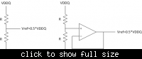
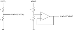
in DDR SDRAM we want to generate Vref as a referenece for 16 input comparators, the nominal value is half the power supply.
i think just use resistor divider is enough for this case, what's benfit to add a buffer stage (unity-gain opamp)? please check the picture.
i don't think there is a speed or loading effects for this case.
any comments?
thanks
 

Attachments

  • vref_gen.png
    vref_gen.png
    8.5 KB · Views: 59

I do not know what it is formally called, but when you have a reference voltage; you do not want it to change even a little bit. If you connect the resistors directly, also if your clock frequency is high enough, clock will feed through your transistors and disturb your reference voltage. Also I believe you do not want to burn a lot of power just to generate references, so I think you are using large resistances making even little current that is fed through transistor deadly (Edit: Well this seems too harsh :D. The term dramatic would be much better. Also if you are designing a RAM I believe you have the tools to do so. Take your time and try it out if buffering improves your performance. If not why waste power :D) to your reference. To keep these distortions very low use a buffer it is a good practice.
 

kemiyun
thanks for your comments.
you are right, i am doing DDR1 PHY interface. i only wish Vref to change with power supply VDDQ, exactly equal to VDDQ/2. i would use large resistors to minimize power.
what do you mean clock frequency? Vref here in my case is DC tied to 16 input comparators for DQ decision making. did you refer to kickback nosie at the data input? but seems not an issue there.so where the distortions come from? in my view, adding an buffer won't help that much but burns more power.
 

I am not sure what I'm referring to :D. But I mean even if theoretically inputs of your comparators are isolated from other input and output at high frequencies this is not true. To keep your reference clean as far as I know the best thing is to control your reference within a feedback loop. By clock I meant your performance specifications. It is more likely to see the coupled high frequency data. But If the fluctuations (I'm not sure if this is true definition :D, what I meant is the ripples and so.) do not disturb your performance specifications, you shouldn't have a worry (But you should be sure that it will work.). But I think it's a good practice to have an isolation layer (It is crucial in ADC's [I mean you should isolate your reference voltage like hell.] but since you just want Vdd/2 I'm not so sure.)
 

The issue is called "loading". Suppose you have a voltage divider to generate Vref. With nothing connected to the midpoint of the resistors, the voltage will be Vref=0.5*Vdd as you have shown. However, when you start connecting a load to the midpoint, the voltage at the midpoint will change, because you are effectively changing the divider ratio. In other words, the bottom resistor has an equivalent resistor in parallel with it which will lower lower the voltage at the midpoint. The buffer helps out in the sense that the + terminal of the opamp does not draw much current from the midpoint of the resistors; therefore, the midpoint voltage stays the same. In addition to this, since V+=V- (due to the negative feedback). The output voltage of the opamp is also Vref. Since the output impedance of the opamp is pretty low, the output voltage will stay at Vref as long as you stay away from the opamp power supply levels. The other constraint is the opamp output current. You can only draw a limited amount of current from the opamp output, so you have to choose the opamp properly to accomplish this.

Best regards,
v_c
 

kemiyun
thanks. what your said is quite reasonable.
we used the later method with opamp to generate, but my colleague see a fluctuation with about 50mV due to cross coupling from other signals

---------- Post added at 16:51 ---------- Previous post was at 16:39 ----------

v_c
thanks for your comments
yes, i will connect the Vref to lots of gate of the NMOS transistors, i assume it's only capacitive loading and since what i care is the DC bias Vref, so i assume can ignore the capacitive loading effect, can I?
my colleague see a fluctuation with about 50mV due to cross coupling from other signals during extracted simulation with the opamp, we use folded-cascoded opamp, he asked me to increase the opamp current to try to minimize the cross-coupled ripple from other metal lines, i was wondering it is a effective method or not.
as you said the output impedance of the opamp is low, i think the output impedance of the standalone opamp is actually quite large, but since it is connected in series-shunt feedback, so the output impedance of the feedback configuration is pretty low, right?
good voltage reference/source should feature small output impedance, it seems i have got the point. but in my specific case, i have no resistive load or i may say my load resistance in parallel with the bottom resistor is huge, so that i may don't need the opamp feedback?
 

... i ... don't need the opamp ...?
You don't need a buffer if you just drive capacitive loads.

If you have empty spaces between your layout blocks, use one or more of them as parallel cap(s) in order to decrease possibly coupled voltage spikes.
 

yes, that's my point. i think the opamp is redundant in this case (no resistive load from midpoint to ground). the fluctuation source has nothing to do with the buffer, most of it comes at the end of the buffer from the nearby toggling metal lines.
Yes, in the layout we have already added more caps loading the line. 50mV ripple is still too much to him, so he said add more current to the buffer, after i read the schematic i think the buffer is redundant, why add more current? that's what i am confused about.
 

Status
Not open for further replies.

Part and Inventory Search

Welcome to EDABoard.com

Sponsor

Back
Top