Sherry1
Member level 3
- Joined
- Apr 4, 2013
- Messages
- 61
- Helped
- 0
- Reputation
- 0
- Reaction score
- 0
- Trophy points
- 1,286
- Location
- Manchester, UK
- Activity points
- 1,810
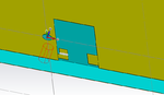
I want to design a Via hole in CST to simulate a through hole in PCB which are used for in Microwave and RF for grounding and thermal relief .
I have three layers
1) Top copper
2) FR4
3) Bottom copper
How do I subtract a cylinder from these layers to make a through Hole.
I have three layers
1) Top copper
2) FR4
3) Bottom copper
How do I subtract a cylinder from these layers to make a through Hole.