Rajinder1268
Full Member level 3
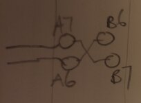
Hi all,
I am using a USB C connector in a design. This is a receptacle that fits into a PCB.
There are 2 x D- and D+ lines. These are connected together as per the guidelines. This is a through-hole connector.
I have attached a picture of the layout of the said connections. One set of tracking is on the Top layer and the other on the bottom layer of my PCB. There is no GND layer where the tracks are crossing.
I wanted to ask if I would need a GND plane for the part where the tracks cross over i.e. between the pins?
Or should I route both tracks on the Top and use X2 vias for one of the tracks and still add a GND plane only under these pins?
My PCB layer is Top (signals), GND, VCC and Bottom (power signals).
Any tips or advice?